Progress Report
Development of a Scalable, Highly Integrated Quantum Error Correction System[3] Scalable Classical-Quantum Interface with Optical/Cryo CMOS Integrated Circuits
Progress until FY2024
1. Outline of the project
Realizing a scalable quantum computer is essential to efficiently transmit huge data communicated between classical and quantum circuits. This necessitates reduction of wiring across the room temperature environment and cryogenic environment. In Item 3, as shown in Figure 1, we will develop an optical/Cryo CMOS integrated circuit that operates at the classical-quantum boundary to realize highly efficient information transmission. As key technologies, we are developing (a) through (b) in Figure 1. This year, we (a) proposed a low-cost qubit control architecture, (b) measured low-temperature characteristics for optical integrated circuits, (c) developed PDKs for Cryo CMOS circuits, and (d) developed design techniques for Cryo CMOS circuits.

2. Outcome so far
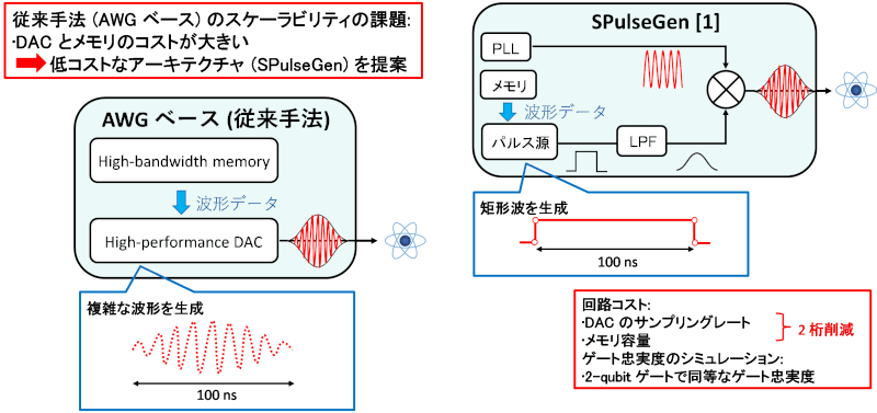
(a)Quantum control architecture for Cryo environment
We proposed a low-cost qubit circuit architecture (Figure 2) enabling sufficient gate fidelity with simpler elements. We also developed design guidelines based on our findings.
(b)Low-temperature Measurement of optical integrated circuits for classical-quantum I/F
Optical integrated circuits showed room-temperature-like switching in liquid nitrogen(Figure3). An evaluation environment for liquid helium conditions was also established.

(c) Development of PDK for Cryo CMOS
We developed modeling techniques based on surface potential theory and machine learning, alongside the industry-standard BSIM4 model. In particular, we extended BSIM4 to incorporate forward body bias effect (Figure 4, left), and demonstrated power optimization through body bias and voltage scaling in ring oscillator designs, all without the need for physical prototyping (Figure 4, right).
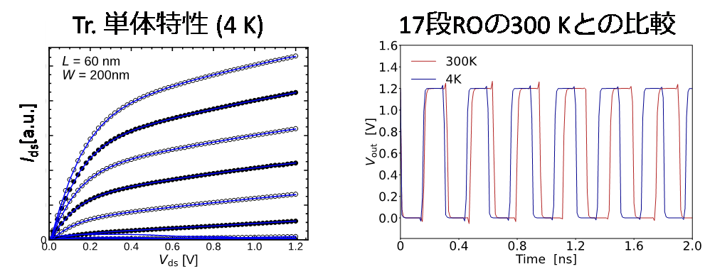

(d) Cryo-Integrated Circuit Design Technology
Random telegraph noise (RTN) in transistors was statistically analyzed using a cryogenic measurement environment specifically built for this study. The experimental results indicate that RTN effects are temporarily suppressed around 100 K; however, they become markedly more pronounced at ultra-low temperatures, such as 3.8 K (Figure 5).

3. Future plans
We will actively consider the integration of each elemental technology and aim to demonstrate and estimate the scalability of the proposed system.