
Research Director: Dr. Shun-ichiro Tanaka
(Chief Research Scientist, R&D Center, Toshiba Corporation)
Research Term: 1993~1998
The Tanaka Solid Junction Project explored the nature and science of hetero-interface formation from the viewpoints of elementary atom dynamics in and around interfaces while pursuing the possibility of actually designing them. The key words are “nanometer dynamics” and “control”. The main objectives were to find ways to understand both the multistep functions and physical states at and around interfaces, and eventually to control the interface reactions and properties while hopefully contributing to the design and fabrication of new materials and components.
Research Results
Direct observation and control of interface formation: Elementary phenomena related to ceramic/metal brazing and bonding were studied by in-situ experiments using a modified TEM that allowed the fabrication and observation of materials with extremely clean surfaces within its chamber. Further, the first-ever observation of the nucleation process has proved that it controls the nanoscopic, dynamic behavior process.
Nature of ceramic/metal interfaces: Nanostructures of the ceramic/metal brazed interface by HRTEM revealed features that explain various mechanical properties. Time-dependent phase changes at the ceramic/metal interfaces were also studied in situ using a newly constructed X-ray diffractometer with a high-temperature stage and imagine plate by which a rapid acquisition of the diffracted pattern was successful during a heating run.
Measured and controlled electron barrier microstructures of metal/Si interfaces: Using a newly constructed ultra-high-vacuum ( 10-10 torr) ballistic electron emission microscope (BEEM) along with an STM, the nanostructures of metal/Si and metal/insulator/Si interfaces were studied in situ. while observing the changing morphology with time it was possible to observe the BEEM current simultaneously, indicating the electronic barrier distributions along the semiconductor-metal and semiconductor-insulator-metal interfaces for the first time.
Nanosized Si dots with interfaces: A nano-sized silicon/metal bilayer dot was also successfully obtained through a surface droplet epitaxy mechanism, which is a self-assembly process.
Residue stress/strain in heterogeneous interfaces: Four new techniques using convergent beam electron diffraction (CBED) within the chamber of a TEM were developed to measure the residual stress/strain distributions around heterogeneous interfaces without any limitation of the materials. The most precise one allows measurements of 25 nanometers by CBED for Si/Silicide interfaces, perhaps the best in the world.
Nanometer bonding and control by an electron beam: Starting with metastable alumina, manometer-sized aluminum particles were made at room temperature within an STM. This was the first time to obtain aluminum particles without an oxide layer.
Theoretical simulations to make interfaces designable: Efforts were made to produce a theory that would allow the design of specific interfaces.
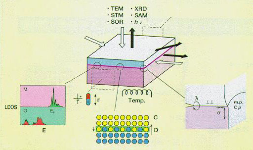
·Phenomena around a hetero-interface and their control
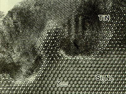
·Lattice image of a ceramic/metal brazed interface
