
Research Director: Dr. Jun-ichi Nishizawa
(Professor, Research Institute of Electrical Communication, Tohoku University)
Research Term: 1981-1986
This project worked toward developing a new generation of semiconductors by combining silicon and gallium arsenic perfect-crystal formation and static-induction control technologies. Static induction transistors (SIT) and thyristors were developed featuring such characteristics as high operating speeds, low noise, low power consumption and large-power handling capacities. Furthermore, crystal photoepitaxy by optical irradiation has been developed as a technology which permits the control of crystal growth with minimal energy, while providing valuable data regarding crystal growth.
Research Results
Photo-excited molecular layer epitaxial growth: The growth of epitaxial films which are necessary for making GaAs compounds semiconducting elements has been realized by low-temperature (350℃), and high-precision (2.5Å) crystal control. This method is applicable for making ultra-high-speed switching circuits and new light-emitting elements. In terms of crystallography, new experimental facts have been obtained regarding the control and elucidation of the stoichiometric structures of GaAs single crystals.
GaAs single crystal: By introducing an arsenic pressure-control method, single crystals having very few lattice defects could be realized. This enables the manufacturing of ultra-high-speed switching elements that are two to three orders faster than ordinary silicon single-crystal elements as well as high-efficiency photo-electric transfer elements.
Electrostatic-induction type photo-sensor: Development of an electrostatic induction transistor which can amplify weak light and convert it to an electric signal. This low-power, low-noise element can detect very weak light (4×10⁻⁶ lux-sec). Super high-performance SITs are produced so thin that disturbances caused by lattice vibrations are virtually insignificant.
Double-gate type thyristor: A basic technique for manufacturing large-power, double-gate, static-induction thyristors has been established. This thyristor has a peak voltage of 1kV, a current capacity of 100 amps and a sub-microsecond switching speed. It enables the miniaturization of electric motors through the use of higher-frequency power supplies.
Ultra high-density SIT integrated circuit: An integrated circuit having a special structure and using a silicone substrate close to a perfect crystal has been manufactured. This IC enables low-power consumption ( less than 10-12 joule), ultra-high-speed switching (less than 10-9 sec) and ultra-low capacity (less than 2×10-12W). This performance is one order higher than conventional circuits.
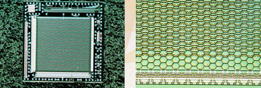
Fig 1: The top view of 64×64 bits static transistor image sensor with newly developed hexagonal pixcell structure.
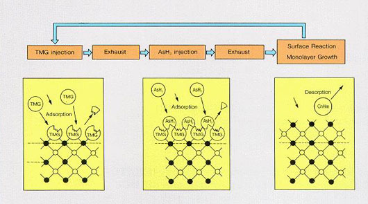
Fig 2: Schematic illustration of the growth mechanism of the GaAs molecular layer epitaxy.
Fig 3: (a) GaAs single crystal grown by the newly developed As pressure controlled Czochralski method. (mirror-like surface)
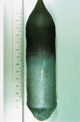
Fig 4: (b) Conventional GaAs crystal
