Research Director: Dr. Shuji Nakamura
(Professor, University of California, Santa Barbara)
Research Term: 2001-2006
The generation of different wavelengths of light using solid-state devices is of extraordinary importance today. For instance, light-emitting diodes (LEDs) offer a very efficient, inexpensive, long-lasting and environmentally friendly way to produce light. Therefore, one of the holy grails of solid-state physics has been to produce light sources over as wide a frequency range as possible.
This is done by fabricating materials with energy band gaps corresponding to the frequencies of desired light and with high quality sufficient to produce a useful intensity. The technology involves producing a substrate with very few defects and then using special equipment to deposit materials epitaxially on top of it in a very ordered manner. This involves a detailed understanding of the science of crystals as well as how to deposit the required materials.
For many years, the materials of choice have been gallium arsenide, gallium phosphide and aluminum gallium indium phosphide. This led to the production of LEDs in the red, orange, yellow, and yellow-green regions. The most sought after device was therefore one that could produce pure green or blue. The reason is simple. Since the wavelength determines how much information can be stored on a CD, for instance, green and blue would allow a much higher information-storage ability. Further, by combining LEDs that emit the primary colors, the production of white light would be possible, leading to the eventual replacement of the very inefficient incandescent and fluorescent bulbs currently in common use. The energy savings would amount to approximately 15 to 20% of the electricity produced in the world today along with corresponding reductions in oil consumption and greenhouse gases.
Shuji Nakamura almost single-handedly realized many breakthroughs in fabrication technology of blue LEDs and lasers. In 1989, he started research on metal organic chemical vapor deposition (MOCVD) of gallium nitride (GaN), a relatively unexplored material. Then in 1993 Nakamura succeeded to make the first blue LED with sufficient output power for applications, and in 1995 the first products in green and blue LEDs using a specially developed quantum-well structure, followed by the first blue laser diode (LD).
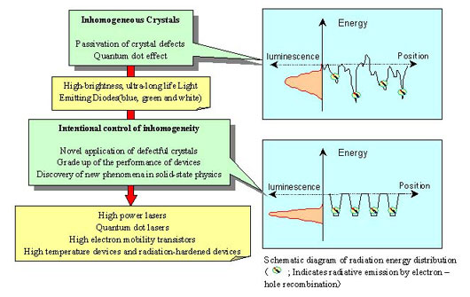
Still, there has remained a basic question of why such good devices can be made with nitride materials having many grown-in dislocations. The lattice mismatch between the sapphire substrate and the gallium nitride layer grown on top of it is too large to produce a defect-free layer. There is a possibility that quantum dots and/or an inhomogeneous crystal structure somehow compensate for the mal-effect of dense dislocations. Elucidating the nature of the quantum dots or inhomogeneous crystal structure of GaN and the interaction of them with dislocations might lead to a better understanding of nitride crystals while leading to a variety of new devices.
Outline of Research
A high-quality, low-dislocation density bulk substrate is necessary to further advance the scientific understanding and control of the inhomogeneous crystal properties of GaN and its alloys. The intentional control of inhomogeneity may present a viable new option to fabricate innovative optical and electronic devices which include high-power, short-wavelength quantum-well semiconductor lasers, quantum-dot lasers, and high electron mobility transistors (HEMT). These devices include novel features, such as improved band structure and the quantum-dot effect, and their properties are dependent on the inhomogeneity in composition, structure and size. The Nakamura lnhomogeneous Crystal Project is pursuing the utilization of these effects through thin-film crystal growth optimization and the fabrication of various solid-state devices. The research is divided into the following three areas:
A special high-pressure, high-temperature reactor is being developed for the fabrication of materials to be used in devices. The main aim is to grow nearly perfect bulk gallium nitride crystals to be used as homogeneous substrates to deposit gallium nitride by MOCVD and MBE (molecular beam epitaxy) with very few, or no, dislocations, instead of the popular sapphire, silicon carbide, and silicon substrates. An effort is also being made to compare various materials with different dislocations, and then to understand their effects.
The second area of research is thin-film growth. The MOCVD and MBE are key technologies for controlling inhomogeneity intentionally. New ideas are being tried for tailoring inhomogeneity, which can cause quantum jumps in device performance. Theoretical simulations of the growth processes help guide the fabrication procedures to make better crystals. Very useful devices, such as LEDs, LDs and electronic devices, are also being developed.
The third area of research is to evaluate the produced materials. An effort is being made to understand the nature and mutual interactions of various inhomogeneities existing in nitride layers and how they affect devices. If this can be achieved, a way will perhaps be found to eliminate, or overcome, the negative effects and to exploit inhomogeneity positively.
The main objective of this project is to explore the nature of inhomogeneity in nitride crystals in a broad sense. The inhomogeneous distribution of indium in gallium indium nitride layers, for example, is of central importance.