
Research Director: Dr. Kingo Itaya
(Professor, Faculty of Engineering, Tohoku University)
Research Term: 1992~1997
Until recently there had been few in situ methods available for the structure determination of an electrode surface in solution at the atomic level. However, in situ scanning tunneling microscopy (STM) became a milestone in electrochemistry for understanding electrochemical reactions with atomic resolution. One of the most important achievements concerning in situ STM was the development by Kingo Itaya of the electrochemical STM with a bipotentiostat, which made it possible to follow a wide variety of electrode processes under potentiostatic conditions. The Itaya Electrochemiscopy Project used mainly in situ STM to investigate various electrochemical reactions on both the atomic and molecular scales.
Research result
Well-defined solid/liquid interfaces:
Well-defined single-crystalline surfaces must be exposed to solution in order to understand surface structure-reactivity relationships on the atomic scale. Efforts have succeeded to produce well-defined, atomically flat surfaces of various metals and semiconductors without either exidation or contamination. An in situ electrochemical etching method has been developed and has become an important general technique for various metals and some semiconductors.
Structures of specifically adsorbed anions:
In situ STM and the complimentary use of in situ STM and ex situ ultrahigh-vacuum techniques, such as low-energy electron diffraction (LEED), have revealed the atmic structures of various adlayers.
Organics on iodine-modified electrodes:
Relatively large organic molecules, such as water-soluble porphyrin and cristal violet, were surprisingly found to form highly-ordered monolayers on iodine-modified Au, Ag, and other electrode surfaces.
Aromatic molecules on Rh(111) and Pt(111):
It was demonstrated that aromatic molecules, such a benzene and naphthalene, form highly-ordered adlayers on bare Rh(111), Pt(111) and other substrates in solution. High-resolution STM images have revealed not only molecular-packing arrangements, but also internal molecular structures adsorbed at different binding sites.
Anodic dissolution processes of metals:
The anodic dissolution of various metals such as Ni, Co, Ag, Au, and Cu has been investigated using in situ STM. The metals in the absence or presence of adlayers were dissolved following a step-selective layer-by-layer mechanism under carefully adjusted conditions in which the dissolution only occurred at the step edges. Such an in situ electrochemical etching method can be used to expose various well-defined metal surfaces in solution.
Semiconductors in solution:
The atomic structures of semiconductor surfaces of Si and GaAs were successfully visualized in solution. Furthermore, it has been established that dynamic processes of etching these semiconductors can be followed by in situ STM.
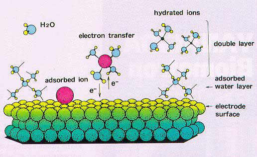
·Schematic model of atomic/molecular interactions at solid/liquid interfaces.
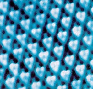
·In situ STM image of a benzene adlayer on a rhodium (111) single-crystalline surface in a hydrofluoric acid solution.
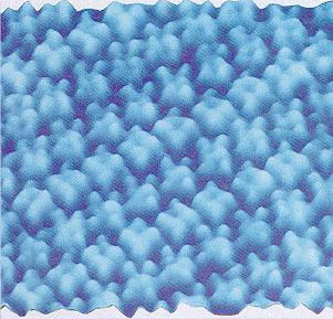
·In situ STM image of a porphyrin adlayer on iodine-modified gold (111) surface in a perchlorate solution.
