Research Director: Dr. Hideo Hosono
(Professor, Materials and Structures Laboratory, Tokyo Institute of Technology)
Research Term: 1999-2004
The Hosono TEAM project explored “today’s stone tools” involving new active properties based on excited electrons in transparent materials as well as novel electronic-active materials.
Research Results
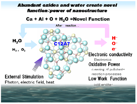
Active function cultivation in an ubiquitous material: 12 CaO·7Al2O3 (C12A7)
Persistent transparent electronic conductor: The light-induced conversion of a typical insulating oxide, 12CaO·7Al2O3, to a persistent transparent electronic conductor was realized. This was the first success to convert a main-group metal oxide to a conductor.
“Dream chemical species”: A micro-porous crystal of 12CaO·7Al2O3 was shown to have the ability to encage an abundant number of O- radicals, considered to be a “dream chemical species” because of its very high reactivity.
Novel applications: Using this unique material, a number of important applications were realized: encaged highly concentrated O-; an O- ion beam; a single crystal; RT-stable electride, electrons as anions; a densely sintered body; a cold electron emitter; flash prints see-through circuits.
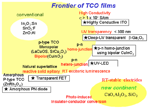
Frontier cultivation of transparent oxide semiconductors:
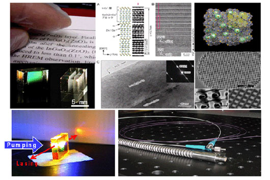
Transparent layered oxychalcogenides: A novel 2D electronic structure by forming stacked alternating positive and negative layers of oxides and chalcogenides was realized. This was done by employing a new technique, named as reactive solid-phase epitaxy, producing an epitaxial thin film. An increased band gap led to transparency.
High-performance transparent transistor: The newly developed reactive solid-phase method was used to fabricate a high-quality transparent thin-film composed of a layered complex oxide, the homologous compound InGaO3(ZnO)n (n = 1-200). Using this material, a high-performance transparent FET was produced with a surprisingly high mobility of 80 cm2/Vs, which is comparable to that in currently used Si.
P-N junctions: Several new devices utilizing P-N junctions formed by transparent oxide semiconductors were realized for the first time. These include a transparent diode based on a P-N homojunction (CuInO2) and a UV-LED utilizing a P-N heterojunction (p-SrCu2O2/n-ZnO).
Extended characteristics: The characteristics of transparent conductive oxides (TCOs) were significantly extended: the lowest resistively record for an ITO (13000 ohm-cm) and a UV-transparent TCO, β-Ga2O3 (transparent down to 250 nm).
Method for laser nano-fabrication in transparent dielectrics:
UV CPA femtosecond system: A UV CPA femtosecond system was realized with very good characteristics (110 fs, 290 nm, 3.5 mJ).
Femto laser nano-fabrication: “Holographic encoding of an interfered fs-laser pulse” was developed, resulting in the fabrication of permanent gratings in transparent materials by two-beam interference from a single femtosecond laser pulse. This process allows the direct writing of an optical integrated circuit inside of transparent dielectrics.
DB color center laser written inside LiF only by photons: A miniatured distributed-feedback color center laser was fabricated inside a LiF crystal by encoding laser-active color centers, waveguides, and micro-gratings working as selective reflection mirrors with fs-pulses. RT-lasering was observed.
SiO2 glass for deep/VUV lasers:
Optical fibres: Optical fibers were developed for deep-UV lasers, such as an ArF excimer laser (193 nm). These fibers have excellent tip characteristics as well as a low optical loss over a wide range of ultraviolet wavelengths and high resistance to UV laser pulses
VUV interaction with SiO2: The interaction of F2 excimer laser irradiation with synthetic SiO2 was elucidated concerning a glass photo-structural change of Si-OH, physical disorder and transparency in VUV.