Progress Report
Development of Integration Technologies for Superconducting Quantum Circuits[3] Research and development of electronics for quantum error correction
Progress until FY2024
1. Outline of the project
In the typical setup of today's superconducting qubit circuits, a qubit chip placed at cryogenic temperatures and microwave electronics operating at room temperature are connected using one or more coaxial cables per qubit. However, due to limitations in space and cooling power of the refrigerator, this method cannot be scaled-up to tens of thousands of qubits. To solve this problem, this R&D Item aims to develop qubit control and readout electronics that operate as close to the qubit as possible and to break through the wiring bottleneck for integration. In this development, the challenge is how to realize a system that efficiently performs quantum error correction within the limited space and cooling capacity of the refrigerator.
This R&D Item focuses on single flux quantum circuits, which can operate at several tens of GHz and have ultra-low power consumption, and NanoBridge FPGAs, which are highly flexible, capable of advanced processing, and have low power consumption, in order to develop low-temperature electronics systems in which they work together.

2. Outcome so far
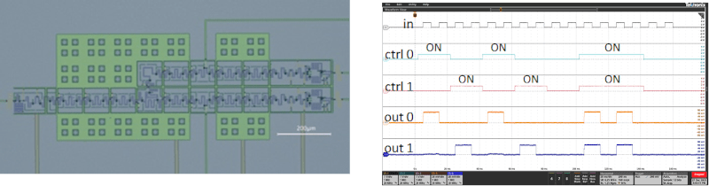
① Demonstration of a single-flux-quantum demultiplexer operating at 14 mK and fabrication of monolithic chip with qubits
Single-flux-quantum (SFQ) circuits have been designed primarily for operation at a liquid helium temperature (4.2 K). However, this research and development aims at operation at the 10-mK stage of a dilution refrigerator, which is the same as that of a qubit, and requires a further reduction in power consumption of conventional SFQ circuits. We established the design guideline for achieving 1/50–1/250 power reduction by lowering the critical current values of the Josephson junctions in the SFQ circuits to 1/10 or less and the driving voltage, considering the changes in device characteristics, and we have created a collection of the circuit elements (such as wire segments and logic gates) called cell library. This fiscal year, we designed a demultiplexer using the developed ultralow-power SFQ cell library and demonstrated the operation in a dilution refrigerator. We also completed the fabrication of monolithic chips that integrated the SFQ demultiplexer and superconductor qubits.
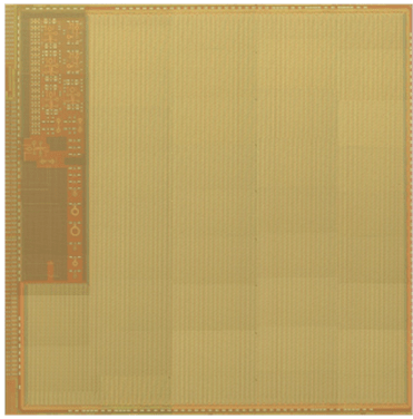
② Completed the fabrication of NanoBridge FPGA for operation at 4 K
We are developing FPGAs that can operate at low temperatures to support a variety of correction algorithms for error correction processing. FPGAs are designed to operate at 4 K. This research project is centered on developing NanoBridge FPGA that can operate at low temperatures, which consumes 1/4 the power compared to commercially available CMOS-based FPGAs operating at room temperature. By last fiscal year, we completed manufacturing the NanoBridge FPGA using standard CMOS process (65nm). This fiscal year, the FPGA have been implemented on low-temperature evaluation boards. As part of the testing, we incorporated a summation-accumulation (MAC) circuit in the FPGA region and found that the 4 K operation can be achieved with significantly reduced power consumption compared to room temperature operation.

3. Future plans
For SFQ circuits, we will test the fabricated monolithic chips for digital control of multiple superconductor qubits.
For NanoBridge FPGA, we will continue characterizing the fabricated chips at low temperatures.
We will also demonstrate cooperative operation of low-temperature electronics using the SFQ demultiplexer and NanoBridge FPGA.