
Research Director: Shoichiro Yoshida
(Managing Director, NIKON Corporation)
Research Term: 1985-1990
High-precision measurement capabilities are at the heart of scientific research and are synergistic with technological development, especially with regards to the present trend towards miniaturization and “nano-engineering.” This project focused on the physical actions and mechanical properties of material in the nanometer region, while investigating new measuring and processing methods.
Research Results
Scanning tunneling microscopes: Several types of scanning tunneling microscopes (STM) were designed: an STM contained within the chamber of a standard scanning electron microscope (SEM); an industrial-type STM for viewing samples from long distances in air: a computer-controlled industrial-type STM; a device comprising a twin-probe STM controlled by a complex mechanism of PZTs and a hinge.
X-ray microscopy: While placing emphasis on the use of both Fresnel zone plates and phase zone plates, X-rays of 1 – 4-nm wavelength were found to be selectively absorbed by biological specimens, making high-resolution x-ray microscope images possible.
Nanometer position-control system: A one-axis stage- positioning mechanism was developed using an actuator, newly designed AC synchronous linear motor and a rolling ball guide which acts like a spring. This system provides an outstanding resolution of 1 nm and a maximum speed of 200 mm/s.
Small-distance positioning systems: A new device employing an ultrasonic linear-motor was developed which uses a segmented PZT bimolf which is 90 degrees out phase.
Nanometer measurement system: A two-wavelength (488 and 244 nm) laser beam interferometer which can eliminate errors caused by air turbulence was developed.
X-ray multilayer mirror fabrication: Since multilayer coatings are necessary for reflecting x-rays in normal-incidence optical systems, the reflectiveness of multilayers made from a wide range of materials were calculated using the Fresnel equation for 1- to 5-nm wavelengths.
Beam processing to make ultra-smooth surfaces: Low-energy (50 eV) Ar-ion/atom beam sputter etching was used to produce atomically smooth surfaces which are applicable as substrates for x-ray multilayer mirrors. This type of processing causes less damage to processed surfaces, making it possible to polish the surface of each layer of x-ray multilayers.
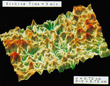
·STM image of etched graphite surface
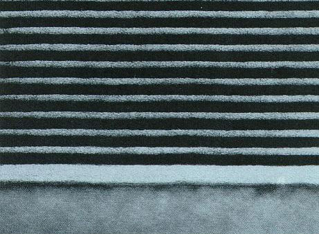
·X-ray multilayer
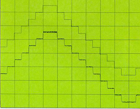
·1nm step responce of mechanical stage
