
Research Director: Dr. Hiroyuki Sakaki
(Professor, Research Center for Advanced Science and Technology, The University of Tokyo)
Research Term: 1988-1993
This project was aimed first at developing new semiconductor fabricationtechnology on the 10 nm level, by which wires and dots and other advancednanometer structures could be prepared with good size and cleanliness control.The project’s goal was then to exploit these structures to create and controlnew quantum mechanical wave states of electrons.
Research Results
Ridge-type quantum wire: A selective MBE method was developedto form a very sharp GaAs ridge structure, from which a nanometer-scalequantum wire was successfully prepared. A sharp and strong luminesceancepeak was observed and has demonstrated the formation of the quantum-wirestate.
Edge-type quantum wire: Electrons in a quantum well can be pulledto the edge region by an electrostatic field to form an edge-type quantum-wirestate. An 80 nm-wide N-AlGaAs/GaAs edge quantum wire was successfully fabricatedby facet growth and has exhibited both transistor action and the one-dimensionalityof electronic motion.
Self-organization of an island-type quantum structure: It was foundthat the deposition of a small amount of InP on latticemismatched GaAsleads to a novel strain-induced coagulation which results in a self-formingInP island and wire structures of sub-100 nm scale.
Ultra-clean etching technology for groove-based quantum structures:An ultra-clean selective etching technology was developed to form cleanand sharp groove structures into GaAs and related materials. Quantum wireswere shown to be formed on the bottom and side regions of the groove.
Resonant scattering transistor: A resonant scattering transistorand other quantum wave phenomena and devices were explored. The resonantcoupling of the two-wave state is controlled by a gate electrode on a double-channelfield-effect transistor geometry to modulate the scattering of electrons.
Novel turnsitile devices: In cooperation with the Technical Universityof Delft, a novel turnstile structure has been developed to control thetransfer of a single electron per on cycle of the gate modulation witha failure rate as small as 10-3.
Electron transport and relaxation in quantum dot structures:Relaxationof electrons in a GaAs quantum dot was studied to estimate two-phonon processesand to disclose prescriptions for highly-efficient quantum dot lasers.Similarly, optical-phonon free transport in coupled box structures waspredicted to exhibit Bloch oscillation, giving rise to a Teraherz oscillationeven at a room temperature.
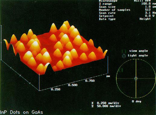
Self-organized InP island structures formed on a GaAssubstrate
