[本文]
Aichi Area

Research Director:
Takashi Miyata
〈Satellite Cluster: Nagano Area, Fukui Area, Yamaguchi Area〉
Energy Innovation Cluster With Advanced Nano-Tools
Theme Overview
The Aichi Area has embarked on research and development through industry-academia-government collaboration such as the Joint-Research Project for Regional Intensive and Knowledge Cluster Initiative.
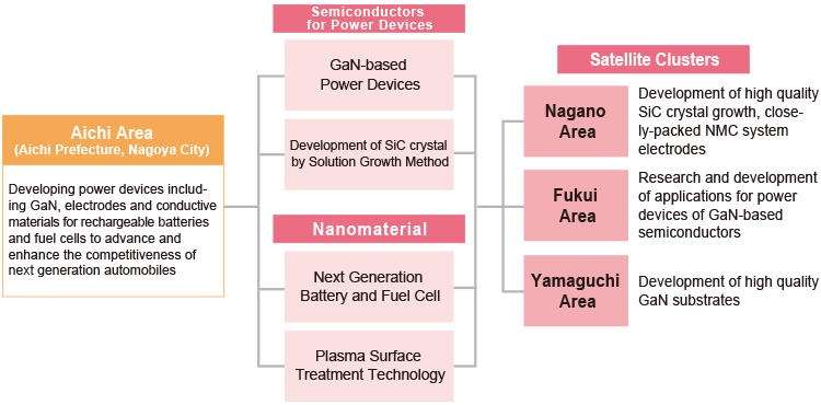
In this Super Cluster Program, under the strategic theme of “construction of a clean and low environmental impact society achievement network”, we promote even greater functionality of nanomaterial and sophistication of nanofabrication that can contribute to reduced energy requirements and environmental impact of what we have developed. Moreover, we develop and advance the social implementation of semiconductors for the next and more advanced generation of power devices, and material for rechargeable batteries and fuel cells to apply them in things such as next generation automobiles, to implement them for a highly efficient energy conservation society, and by extension to achieve a vital and sustainable society.
Plan
The Aichi Area core cluster, with the Aichi Science & Technology Foundation as the core organization, will construct a close collaboration system with related organizations such as Aichi Prefecture, Nagoya City, Nagoya University, Nagoya Institute of Technology and the like. Knowledge Hub Aichi in Aichi Prefecture and the Plasma Center for Industrial Applications in Nagoya City will also be used as cores for R&D and industrialization to maximize program effects on local industries.
As research themes, we will target the following: for power device semiconductors, we will improve the functionality of GaN-based materials and apply them in devices, and establish the technology for low defect SiC crystal substrate fabrication; for nanomaterials, we will commercialize next generation cell materials, and lightweight and high hardness materials for vehicles with advanced plasma technology. We will promote them combining crystal/material analysis and area businesses.
For the development of GaN/GaN-based devices, the Yamaguchi Area satellite will develop GaN substrate, and the Aichi Area core cluster will develop GaN wafers for power devices by laminating epitaxial film on the substrate.
Then the Fukui Area satellite will develop new power devices using the wafers. Each will bring its own technological forte to research and develop concurrently toward one target, increasing the speed of research and development. Moreover, SiC crystal using a solution growth method, and next generation batteries and fuel cells will also be jointly researched and developed through the collaboration of the Aichi Area core and the Nagano Area satellite.
Toward Social Implementation
Working toward social implementation, over 40 corporations will participate in each theme under each university research leader to carry out joint research and commercialization.
We will fully use the collaboration conference and joint research promotion committee to share information and manage progress to achieve the intended purpose.
Aichi Core Cluster
Energy Innovation Cluster With Advanced Nano-Tools
Purpose
- Strengthen international competitiveness of the Aichi Area in automobiles and electronics by establishing a wide-range collaboration among core satellites
- Installation of next generation fuel cells and rechargeable batteries, and implementation of social systems including smart grids
Overview
- Research and development of applications for power devices of GaN-based semiconductors

- GaN-based semiconductor application devices
- Research and development concerning high-quality development techniques and evaluation techniques of SiC single crystal by solution growth method
- SiC crystal development / Single crystal evaluation
- Research and development of increased capacity and safety technology of electrodes and conductive materials for next generation rechargeable batteries and fuel cells
- (Crystalline) electrode material for batteries / Conductive material for fuel batteries / High concentration CNT ink (dispersion processing)
- Research and development concerning material application of nanomaterial synthesis and surface treatment technology with advanced plasma
- Atmospheric pressure plasma / High durability precision metal mold (nitriding)
Participating Organizations
- Universities
- Nagoya University, Nagoya Institute of Technology
- Public Research and Development Institute
- Aichi Center for Industry and Science Technology,
Nagoya Industries Promotion Corporation Plasma Center for Industrial Applications - Corporations
- Toyota Motor Corporation, Aisin Seiki Co., Ltd., DENSO Corporation, Sumitomo Chemical Company, Limited, Daido Steel Co., Ltd, Taiyo Kagaku Co. Ltd., Toyota Industries Corporation, and others
Adoption Subjects
- Aichi Area
- Kyoto Area