HOME > Events > 2013 MRS Fall Meeting & Exhibit JST booth features a variety of novel materials
Events
3-5 December, 2013
2013 MRS Fall Meeting & Exhibit
JST booth features a variety of novel materials
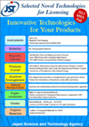
During the 2013 MRS Fall Meeting & Exhibit, JST will have our booth at MRS exhibition in Boston from December 3 to 5. JST booth will feature a variety of novel materials, covering from Batteries, Magnetic device, Photonic crystal, Cavity QED, Quantum Dot, Superconductor, Oxides, and Organic Materials to Instruments, which JST experts have strictly selected from over 3000 patents available for licensing. We are happy to welcome MRS participants at our booth.
* JST undertakes licensing activities in order to facilitate commercialization of the innovative research outputs originating from universities and JST funding programs.
* JST undertakes licensing activities in order to facilitate commercialization of the innovative research outputs originating from universities and JST funding programs.
Date : Tue Dec 3, 2013 - Thu Dec 5, 2013
Location: Hynes Convention Center, Boston, MA
JST Booth No. : 204
Event Web Site:
Location: Hynes Convention Center, Boston, MA
JST Booth No. : 204
Event Web Site:
Catalogue at MRS Fall Meeting/Exhibit
- 2013 MRS Fall [7.0MB]
- Back number
2012 MRS Fall [6.8MB]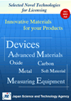
- Back number
2011 MRS Fall [29.7MB]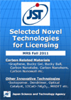
| SN | Category | Technology (Link to detailes PDF) | Inventor (Link to Researchmap) | Patent |
|---|---|---|---|---|
| 2012-58 | INSTRUMENTS | Nano-suit: a thin-layer of amphiphilic solution to observe the fine structure of living organisms in FE-SEM | Takahiko HARIYAMA (Hamamatsu University School of Medicine) |
WO2013/035866 |
| 2013-17 | INSTRUMENTS | Magnetic Field Imaging using Magnetic Field Reconstruction Software | Kenjirou KIMURA (Kobe University) |
WO2008/123432 |
| 2013-16 | INSTRUMENTS | Electrically-induced micro-bubble knife enables ablation and injection for biomedical applications | Yoko YAMANISHI (Shibaura Institute of Technology) |
WO2013/129657 |
| 2013-18 | BATTERIES | Na+ Rechargeable Batteries using Novel Na3PS4 Glass-Ceramic Electrolytes | Akitoshi HAYASHI (Osaka Prefecture University) |
WO2013/015321 |
| 2013-13 | MAGNETIC DEVICES | Half-Metallic Films and Magnetoresisive Devices | Koichiro INOMATA (Tohoku University) |
WO2007/126071 WO2004/055906 |
| 2013-14 | MAGNETIC DEVICES | Giant Tunnel Magneto-resistance (TMR) Device with Crystalline MgO Barrier | Shinji YUASA (AIST) |
WO2005/088745 WO2006/022183 |
| 2013-15 | MAGNETIC DEVICES | CPP-GMR Devices Using Synthetic Antiferromagnet | Koichiro INOMATA (Tohoku University) |
WO2004/068607 |
| 2013-07 | PHOTONIC CRYSTAL | Ultra-High-Q Nanocavity using Two-dimensional Photonic Crystals | Susumu NODA (University of Kyoto) |
WO2003/081304 WO2003/081305 WO2004/053549 |
| 2013-08 | PHOTONIC CRYSTAL | Surface -Emitting Diode Laser using Two-dimensional Photonic Crystals | Susumu NODA (University of Kyoto) |
WO2004/086575 |
| 2013-09 | PHOTONIC CRYSTAL | Conversion of Broadband to Narrowband Energy using Two-dimensional Photonic Crystals | Susumu NODA (University of Kyoto) |
- |
| 2013-10 | QUANTUM ENTANGLEMENT | Non-degenerate Polarization-entangled Photon Pair Generation Device | Keiichi EDAMATSU (Tohoku University) |
WO2009/093391 |
| 2013-12 | QUANTUM ENTANGLEMENT | Photon Pair Generation in Biexcitonic Cavity QED and Device | Hiroshi AJIKI (Osaka University) |
WO2007/094094 WO2005/103810 |
| 2013-11 | OPTICAL MANIPULATION | Quantum dot manipulating method and quantum dot production/manipulation apparatus | Tadashi ITOU (Osaka University) |
WO2005/087654 |
| 2013-01 | SUPER-CONDUCTOR | Magnesium Diboride (MgB2) as superconducting Materials | Jun AKIMITSU (Aoyama-Gakuin University) |
WO2002/055435 |
| 2012-01 | SUPER-CONDUCTOR | Electro-conductive & Transparent Nano-porous Compound C12A7 | Hideo HOSONO (Tokyo Institute of Technology) |
WO2001/079115 WO2003/050037 WO2003/033406 WO2005/000741 WO2005/077859 WO2003/089373 |
| 2013-04 | SUPER-CONDUCTOR | Iron-Based New Superconductors | Hideo HOSONO (Tokyo Institute of Technology) |
WO2009/119216 |
| 2013-02 | OXIDES | Novel Materials ; BaTiO3-XHX (0<x<0.8) | Hiroshi KAGEYAMA (Kyoto University) |
WO2013/008705 |
| 2013-03 | OXIDES | Cesium Lithium Borate (CsLiB6O10, CLBO) Single Crystals for Ultraviolet Light Generation | Yuusuke MORI (Osaka University) |
- |
| 2013-05 | ORGANIC MATERIALS | Ladder π-Conjugated Materials for OLED | Shigehiro YAMAGUCHI (Nagoya University) |
WO2005/044826 WO2005/087780 |
| 2013-06 | ORGANIC MATERIALS | Bucky Gel Actuator | Kinji ASAKA (AIST) |
WO2005/057772 |
Explore Technologies
Quick Links JST Patent List
Contact
Japan Science and Technology Agency
Department of Intellectual Property Management
Science Plaza
5-3, Yonbancho, Chiyoda-ku
Tokyo 102-8666
JAPAN
Phone: +81-3-5214-8486
Fax: +81-3-5214-8417
Email: 
Copyright(c) JAPAN SCIENCE AND TECHNOLOGY AGENCY. All rights reserved.