Progress Report
Fault-tolerant Quantum Computing with Photonically Interconnected Ion Traps[4-2] R&D for Cloud Quantum Computing
Progress until FY2024
1. Outline of the project
We will implement automation and remote operation technologies that are essential for the cloud computing of ion trap quantum computers and create an environment where small-scale quantum computers can be used remotely by educational institutions and other organizations. To this end, we will greatly improve the reliability of basic ion control technology and enable all series of operations in experiments (e.g., ion loading, laser cooling, gate operation, etc.) to be performed remotely. In addition, as fundamental technology development to improve the performance of the cloud-based ion trap quantum computer, we will conduct ion transport experiments to integrate the ion trap module and two-dimensional ion array experiments to expand the number of qubits.
2. Outcome so far
We are conducting research and development toward the realization of quantum computing using ytterbium ions (Fig. 1). In this study, we have developed a technique to selectively introduce a specific isotope (171Yb⁺) of ytterbium ions into an ion trap and maintain it stably. In our quantum computing experiments using ions, two energy states of the ground state of ytterbium ions are used as qubits. In this experiment, we used external light irradiation to detect which of the two energy states the ion is in. As a result, we succeeded in detecting the qubit state with an error rate of 6 %. Based on the state detection, we succeeded in observing Rabi oscillations by irradiating microwaves externally (Fig. 2). Furthermore, we have succeeded in observing stimulated Raman transitions using light (355 nm pulsed laser light). We plan to proceed to two-qubit gates and cloud connection tests.


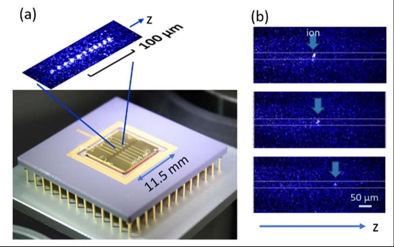
We perform ion transport experiments using a surface-electrode trap consisting of multiple trapping regions as shown in Fig. 3 (a). Ion position is manipulated by varying voltages applied to these electrodes. Figure 3(b) shows snapshots of the ion transport experiment. To reduce the ion heating, the ion is gradually accelerated and decelerated at the start and end points. In this way, 10,000 shuttling were successful. In addition to the development of trap electrodes, it is important to develop a voltage control system that enables fast transport.
Working with manufacturers, we developed a multichannel FPGA-based voltage control system that improved the sampling rate by two orders of magnitude and the output voltage by five times compared to a commercially available system.
3. Future plans
We will implement two-qubit quantum gates, improve its accuracy, and implement a relatively simple algorithm so that the quantum gate algorithm experiment can be operated. Ion transportation technique is of significance because it determines the computation time of quantum computers. The ion transport technique is important because it determines the computation time of quantum computers. We will improve the electrical circuit to achieve faster transport and expand the control system for the large-scale ion trap quantum computer