Progress Report
Fault-tolerant Quantum Computing with Photonically Interconnected Ion Traps[1] Research and development for photonic interconnects of ion traps
Progress until FY2024
1. Outline of the project
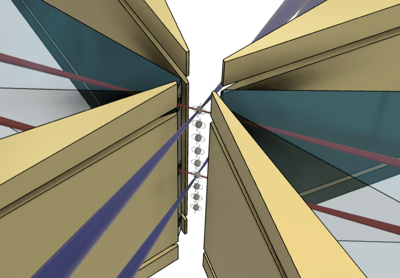
In this research, we aim to realize a large-scale quantum computer using ion traps by developing a "quantum photonic interconnect" that links multiple traps via photons. Central to this effort is a novel device integrating a micro-optical resonator and a linear ion trap. The resonator enables strong ion-photon coupling, while the linear trap stably confines multiple ions in a line (see figure below). Quantum photonic interconnects become feasible only when both functions are achieved within a single device.
We also work on other themes such as enhanced ion-photon coupling using Ba+ ions and development of an optical cavity using semiconductor mirrors.
2. Outcome so far
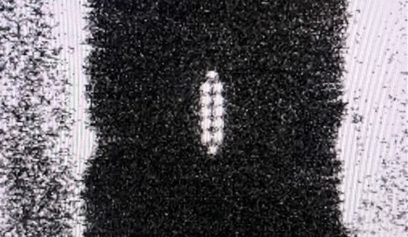
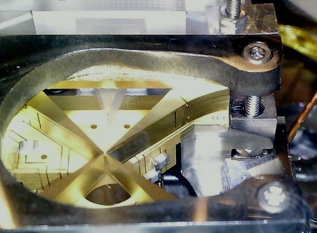
In FY2022, we successfully trapped calcium ions using the developed ion trap (Fig. 2), and in FY2023, we evaluated its characteristics and confirmed the effectiveness of motion control techniques. In FY2024, we advanced the design and fabrication of a second-generation ion trap integrated with a micro-optical resonator (Fig. 3), and nearly completed preparations for the experimental setup. These developments have laid a solid foundation for the next phase of resonator integration.
We continued efforts to integrate optical cavities with ion trap chips using semiconductor mirrors. In FY2024, we evaluated the performance of a microcavity using fiber mirrors based on the structure developed last year. As a result, we achieved a finesse of 100,000 (Fig. 4), marking a significant step toward cavity integration.

3. Future plans
We integrate optical cavities in ion traps and aim to couple single ions to the optical cavities.