Progress Report
Fault-tolerant Quantum Computing with Photonically Interconnected Ion Traps[4-1] Fabrication and evaluation techniques of high-performance ion traps
Progress until FY2024
1. Outline of the project
To realize ion-trap modules for photonically-interconnected ion-trap quantum computing, novel approaches must be implemented to the ion traps. The approaches include ion-photon quantum interconnect, microwave-based qubit control and quantum encoding to phonons. The goal of our R&D theme is to develop ion-trap fabrication and evaluation techniques to enable these approaches. We also try to join other ion-trap research groups in Japan to the development cycle of the fabrication and evaluation by distributing more versatile trap samples and by obtaining feedback. The project consists of three trap-evaluation groups using Ca+(calcium ion), Yb+(ytterbium ion) and Ba+(barium ion).
2. Outcome so far
While 3D ion traps provide stronger ion confinement and immunity to field disturbances by mirrors for the ion-photon interconnect, planar traps have an advantage of accommodating complex functions such as junctions. We are developing both traps in parallel.
A 3D ion trap consisting of AlN substrates with good thermal conductivity(Fig.1(a)) is about to be deployed to ion trap experiments. A process of assembling chip electric parts in a cleaner way has been developed for improving the vacuum performance. The operating parameters for the selective laser etching method has been successfully optimized to fabricate trap structures onto fused silica substrates (Fig.1(b). The first generation of the planar trap assembled in a vacuum package has been deployed to four groups to evaluate the performance. The 2G planar trap with improved surface precision is ready for trapping, and the 3G planar trap with improved motion controllability is ready for fabrication.
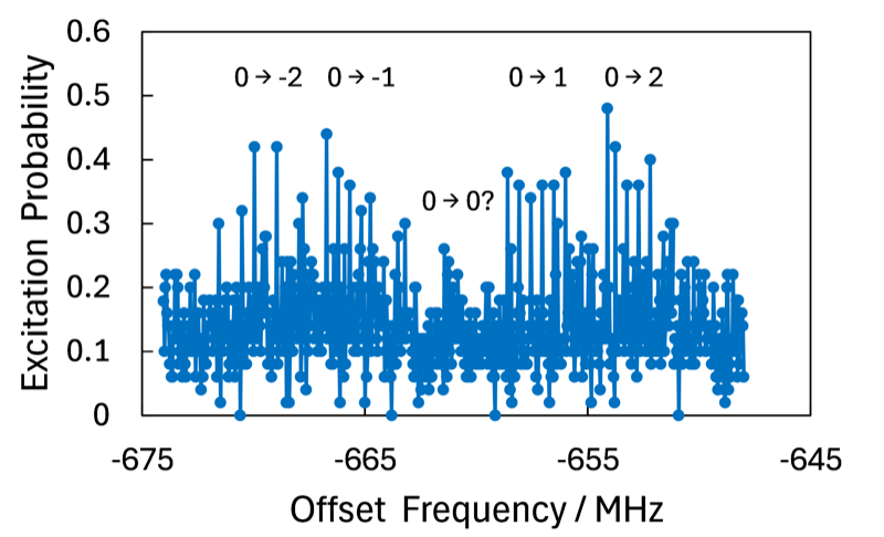
The Yb+ group for 3D trap evaluation develops cooling technique for 171Yb+ to the Lamb-Dicke parameter of 1.5 and succeeded in detecting the magnetic-field-insensitive mF=0 to 0 component toward long coherence time in the quantum computation.
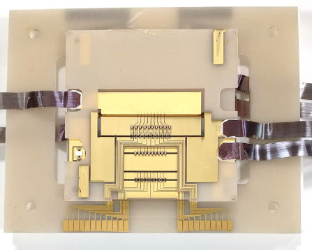
The Ba+ group has designed and fabricated a trap system including an atomic source, laser beams, imaging system, and magnetic field-applying coils (Fig. 3). They successfully developed a high-voltage rf driver consisting of common electronic components that allow simpler implementation than helical resonators. A new laser light source at 533 nm has also been constructed for isotope-selective ion loading. They also proceeded with the fabrication of a prototype vacuum package for a compact ion trap module.

3. Future plans
The traps will be supplied to the groups for evaluation. Our goal is to develop fabrication and evaluation techniques to realize ion-trap modules for photonically connected ion trap QC in collaboration with project groups and companies in Japan.