- JST Home
- /
- Strategic Basic Research Programs
- /
 CREST
CREST- /
- Research Director/
- Fundamental Technology for Semiconductor-Device Structures Using Nanomaterials/
- [Nano-material semiconductors] Year Started : 2023
[Nano-material semiconductors] Year Started : 2023
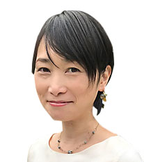
Ayumi Ishii
Development of novel photofunctional devices based on one-dimensional helical nanomaterials with organic-inorganic hybrid
Grant No.:JPMJCR23A1
Research Director
Ayumi Ishii

Associate Professor
Faculty of Science and Engineering
Waseda University
Collaborator
| Tetsuaki Itou | Professor Faculty of Advanced Engineering Tokyo University of Science |
| Shinnji Tanaka | Senior Researcher Interdisciplinary Research Center for Catalytic Chemistry National Institute of Advanced Industrial Science &Technology |
| Tatsuki Tahara | Senior Researcher Radio Research Institute National Institute of Information and Communications Technology |
Outline
This project will establish fundamental technologies for new photofunctional functions and devices based on one-dimensional helical inorganic nanomaterials with unique electronic and spin states, which is controlled by organic-inorganic hybrid structures. The electronic states and optical functions induced by one-dimensional helical arrangements with broken spatial inversion symmetry and strong spin-orbit interactions (circularly polarized light detection, bulk photovoltaics, and photocurrent-induced magnetism) will be used to develop next-generation optical semiconductor devices (multi-dimensional optical imaging system, ultra high-power solar cells, and ultra energy-saving information processing devices).
Toshiaki Kato
Development of graphene-based standard quantum limit amplifier with interface-controlled direct growth method
Grant No.:JPMJCR23A2
Research Director
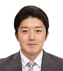
Toshiaki Kato

Professor
Graduate School of Engineering
Tohoku University
Collaborator
| Tomohiro Otsuka | Associate Professor Advanced Institute for Materials Research, Research Institute of Electrical Communication Tohoku University |
| Kouichi Semba | Project Professor Graduate School of Science The University of Tokyo |
| Fumiki Yoshihara | Professor Faculty of Science Tokyo University of Science |
Outline
In this study, we attempt to develop basic technology for fabrication of graphene-based standard quantum limit (SQL) amplifier by improving our direct fabrication method of graphene devices. Since the SQL amplifier can amplify a signal with keeping ultra-low noise level, it can be expected to be utilized in future quantum devices such as a quantum computer by drastically improving SQL amplifier performances with graphene.
Masaharu Kobayashi
Nanosheet oxide semiconductor for 3D integrated memory devices
Grant No.:JPMJCR23A3
Research Director
Masaharu Kobayashi

Professor
Institute of Industrial Science
The University of Tokyo
Collaborator
| Mutsunori Uenuma | Group Leader Sensing Technology Research Institute National Institute of Advanced Industrial Science and Technology |
| Yukiharu Uraoka | Professor Graduate School of Science and Technology Nara Institute of Science and Technology |
Outline
In this research, we aim at developing atomic layer deposition process for nanosheet oxide semiconductor, exploring physics and interface properties in nanosheet oxide semiconductor devices, and demonstrate 3D integrated memory devices. Experts of material/process, device, characterization, theoretical calculation in the field of oxide semiconductor and nanoelectronics collaborate and achieve the research goals.
Taishi Takenobu
Ultra-high-density carrier control in two-dimensional materials
Grant No.:JPMJCR23A4
Research Director
Taishi Takenobu

Professor
Graduate School of Engineering
Nagoya University
Collaborator
| Wen Hsin Chang | Senior Researcher Semiconductor Frontier Research Center National Institute of Advanced Industrial Science and Technology |
| Kaori Hirahara | Professor Graduate School of Engineering Chiba University |
| Mina Maruyama | Assistant Professor Institute of Pure and Applied Sciences University of Tsukuba |
| Yasumitsu Miyata | Group leader The International Center for Materials Nanoarchitectonics (MANA) National Institute for Materials Science |
Outline
We will establish area- and type-selective high-density carrier doping techniques for two-dimensional materials, such as monolayers and in-plane and out-of-plane heterostructures, focusing on transition metal chalcogenides. Based on these techniques, we aim to establish the sciences of metal/semiconductor junctions and PN junctions in two-dimensional materials and to realize functional devices based on them.
Katsuhiro Tomioka
3D integrated quantum electronics and circuits using vertical semiconductor nanowire array
Grant No.:JPMJCR23A5
Research Director
Katsuhiro Tomioka

Professor
Graduate School of Information Science and Technology
Hokkaido University
Collaborator
| Koji Inoue | Professor Graduate School and Faculty of Information Science and Electrical Engineering Kyushu University |
| Kohei Hamaya | Professor Graduate School of Engineering Science The University of Osaka |
Outline
Based on III-V nanowires and their heterostructures, we develop novel 3D integrated circuit technologies including new devices, processes, and circuit architecture toward realization of ultra-low power electronics and their society.


