- JST Home
- /
- Strategic Basic Research Programs
- /
 ACCEL
ACCEL- /
- R&D Projects/
- Completed/
- Development of Flexible Nitride Semiconductor Devices with PSD
Development of Flexible Nitride Semiconductor Devices with PSD
|
| Brochure PDF |
Research Director
Hiroshi Fujioka
(Professor, Institute of Industrial Science, The University of Tokyo)
1984 B.S., The University of Tokyo
1984 Engineer, Fujitsu Limited
1995 Ph.D., University of California at Berkeley
1995 Research Associate, University of California at Berkeley
1996 Research Associate, The University of Tokyo
1998 Assistant Professor, The University of Tokyo
1999 Associate Professor, The University of Tokyo
2004 Professor, Institute of Industrial Science, The University of Tokyo
Program Manager
Akira Usui
(ACCEL Program Manager, Japan Science and Technology Agency)
1970 BA in Chemical Engineering, Tohoku University
1970 NEC Corporation
1997 Ph.D. University of Tsukuba
2002 Furukawa Company Ltd.
2016 ACCEL Program Manager, JST
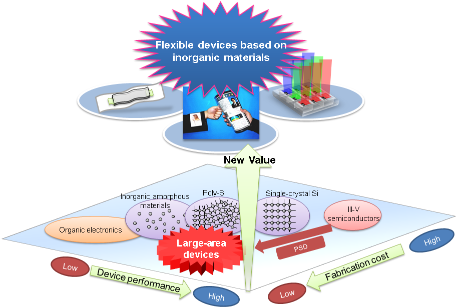
Outline of R&D Project
Under the previous CREST project, we developed a new low temperature growth technique for high quality nitride semiconductors called PSD.*1)The use of PSD allows us to fabricate various nitride semiconductor devices on large-area substrates that cannot survive high temperature processing. In fact, we succeeded in fabrication RGB full color LEDs on amorphous substrate with the use of this technique.
In this ACCEL project, we will integrate a LED array with its driving circuits based on the nitride semiconductors on a flexible substrate to demonstrate feasibility of our technique for display applications.
*1) PSD (Pulsed Sputtering Deposition):
A kind of sputtering thin film deposition method which offers high quality epitaxial films even at low substrate temperatures