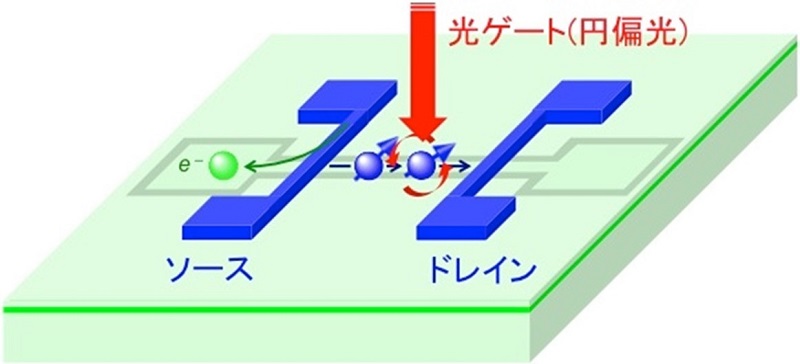
スピン偏極トランジスタ素子
廣畑 貴文(英国ヨーク大学)
発明のポイント
- ・ 円偏光を用いてスピン偏極電流を制御するという全く新しいスピン偏極トランジスタを提案。
- ⟷ 従来の電界効果トランジスタ:電場や磁場を用いたゲート制御
- ・ 円偏光の侵入長は半導体伝導経路上の膜厚及び入射角によって制御可能。
- ・ 半導体中を流れるスピン偏極電流を厳密に変調制御可能。
- ・ 円偏光の波長を半導体のバンドギャップに一致させることで、高効率な制御が可能。
発明の概要
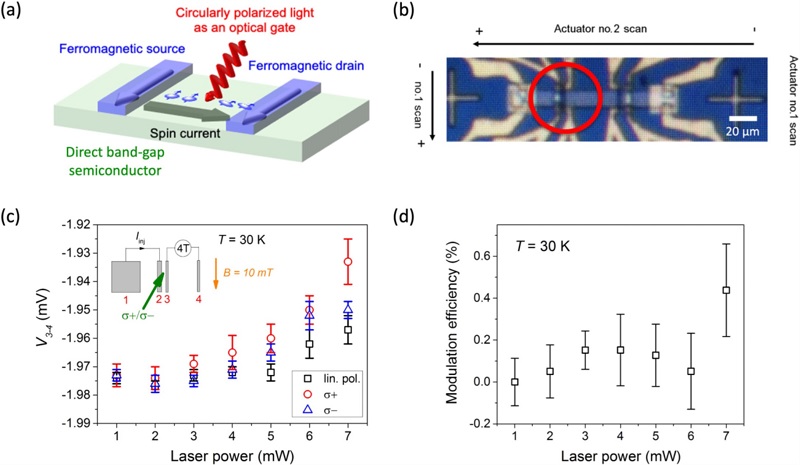
- (a) Schematic of the optical gating in nonlocal spin injection devices.
- (b) The optical micrograph of our device in the optical cryostat used for the time-resolved Kerr measurements. The red circle indicates the region of the circularly polarized light excitation.
- (c) Nonlocal voltage (measured between the contacts 3 and 4 with Iinj = −100 μA at 30 K) with the clockwise (red) and the counterclockwise (blue) circular polarizations and the linear polarization (black).
- (d) Optical modulation efficiency, defined as the percentage ratio of the difference and the sum of the nonlocal voltages with the clockwise and the counterclockwise circular polarization, (V3−4,σ+ −V3−4,σ−)/(V3−4,σ+ +V3−4,σ−), against the laser power.
従来技術との比較・優位性
- ・ スピン・トランジスタでは、電場もしくは磁場を用いたゲートが一般的。
→ 光ゲートは世界初の提案。
| 従来技術 | 本発明 | |
|---|---|---|
| 伝導経路厚 | 数10nmで固定 | 制御可能 |
| ゲート長 | 22mm | 無制限 |
想定される用途
- ◎ 小型化可能な構造を有するトランジスタ素子
- ◎ 円偏光のスイッチング速度がゲート変調速度にそのまま依存することから、現在のCOMS素子と同等以上の速度で動作可能
- ◎ 面内スピントランジスタや縦型ナノピラー等の強磁性体/半導体ハイブリッド構造におけるゲート制御としても適用することができる
ライセンス可能な特許
発明の名称:スピン偏極トランジスタ素子
国際公開番号:WO2014/027555
登録番号:特許第5569851号(91KB)、米国9190500(956KB)
