Research
- Research Theme
- “Si Nano-Wire Solar Cells”
This is research of silicon nano-wire solar cells that improve the conversion efficiency of silicon solar cell to more than 30%. Three teams are formed under the Research Director to conduct research and development. To achieve the aim of this research, we combine bandgap engineered nano-wire solar cells and high efficiency Si heterojunction solar cells as a tandem system.
- Research Team
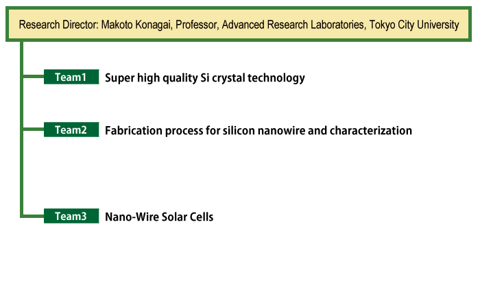
Group1-1 Super high quality Si crystal technology
Group2-1 Metal assisted etching and innovative process
Group2-2 Self organization
Group2-3 Fabrication of nanowire thin films
Group3-1 High efficiency Si solar cells
Group3-2 Coupling structure
Group3-3 Optical-Confinement and Device-Fabrication techniques
- Research Plan
Overall
Plan of each group
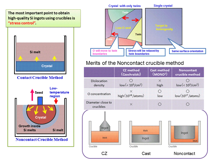
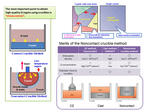
 Super high quality Si crystal technology
Group1-1 Super high quality Si crystal technology

Kazuo Nakashima
Professor, Graduate School of Energy Science, Kyoto University- 1. Objectives
- The development of an innovative method which enables to grow high-quality Si ingots, and the supply of high-quality Si wafers for solar cells.
- 2. Methods
- Basing on the “Noncontact Crucible method” developed by our laboratory, we develop innovative method realizing high-quality Si ingots.
- 3. Goal
-
- (1) Improvement of quality: dislocation-free, low oxygen concentration, low-content carbon, high-purity, quite-homogenous crystals
- (2) large-scaling of ingots, reducing the production cos
 Fabrication process for silicon nanowire and characterization
Group2-1 Metal assisted etching and innovative process

Shinsuke Miyajima
Associate Professor, Graduate School of Science and Engineering, Tokyo Institute of Technology- 1. Objectives
- Development of silicon based nanowires with a bandgap of 1.7 eV and good optical confinement, and core technologies for nanowire solar cells.
- 2. Methods
-
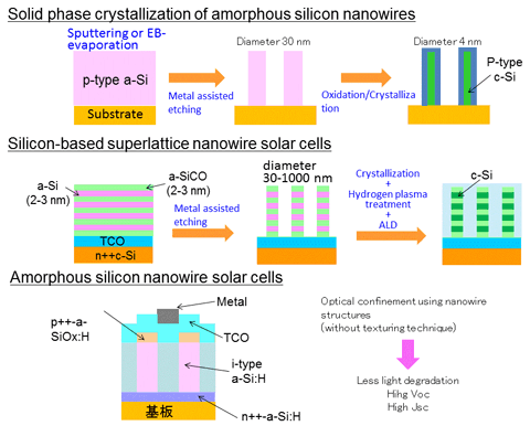
- (1) Solid phase crystallization of amorphous silicon nanowires
We realize Silicon nanowires with 4 nm diameter by solid phase crystallization of amorphous silicon nanowires which are fabricated by metal-assisted chemical etching using silica nanoparticle - (2) Silicon-based superlattice nanowire solar cells
We develop silicon-based superlattice nanowires with diameters less than 1μm. The nanowire structure enhances the optical confinement of the bandgap controlled superlattices - (3) Amorphous silicon nanowire solar cells
We develop high efficiency amorphous silicon (bandgap : 1.7 eV) solar cell by combining thin-film silicon solar cell technologies and nanowire technologies.
- (1) Solid phase crystallization of amorphous silicon nanowires
- 3. Goal
-
- (1) Development of silicon nanowires with 4 nm diameter
- (2) Development of silicon-based superlattice nanowires with diameters less than 1μm
- (3) Realization of high efficiency amorphous silicon solar cells.
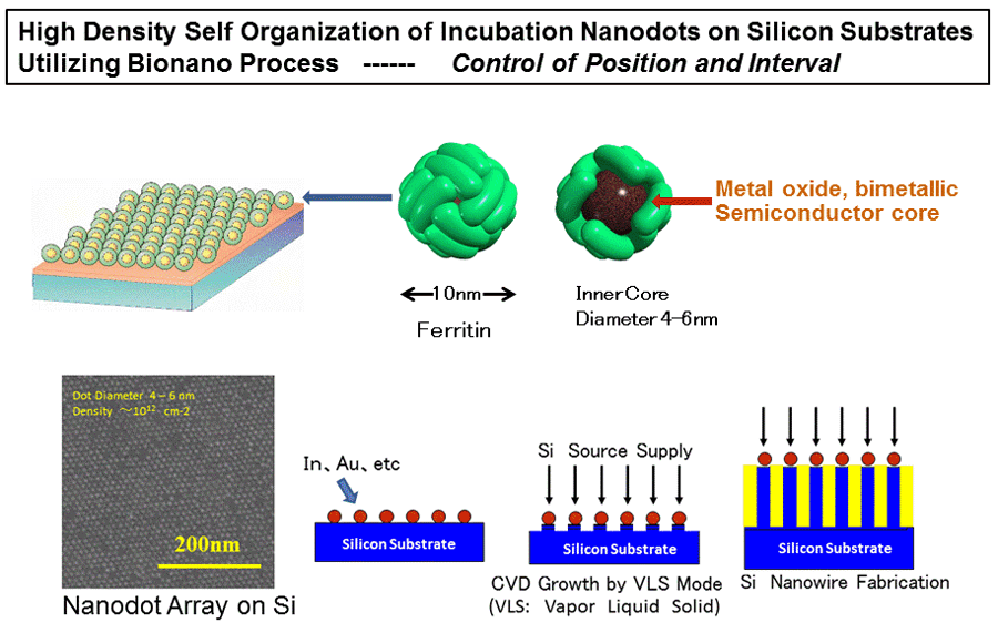
Group2-2 Self Organization
- 1. Objectives
- Fabrication of silicon nano-wires using bionano template and application to heterostructure solar cells
- 2. Methods
-
- (1) Fabricate silicon nano-wires on silicon substrates by bionano process using ferritin molecules
- (2) Characterize silicon nano-wires in the viewpoint of optoelectronic properties
- (3) Make heterostructure of silicon nano-wires and silicon substrates
- 3. Goal
-
- (1) Development of technologies fablicationg silicon mano-wires (5 – 10 nm diameter) on silicon substrates
- (2) Application to high efficiency silicon solar cells in heterostructures with nanowires

Group2-3 Fabrication of Nanowire Thin Films

Noritaka Usami
Associate Professor, Institute for Materials Research, Tohoku University- 1. Objectives
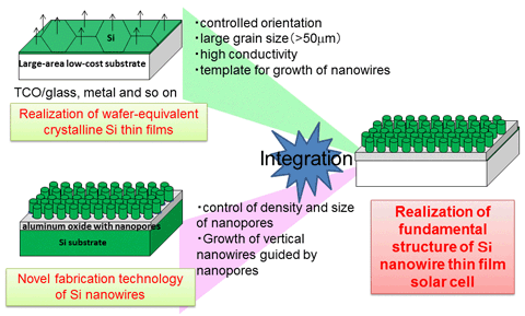
- Realization of fundamental structure of Si nanowire thin film solar cell by combining novel fabrication technology of Si nanowires and wafer-equivalent crystalline Si thin films
- 2. Methods
-
- (1) Develop a novel fabrication technology of Si nanowires embedded in a dielectric matrix
- (2) Develop crystal growth process of wafer-equivalent of crystalline Si thin films on large-area low-cost substrates based on metal-induced layer exchange process
- 3. Goal
-
- (1) Development of novel fabrication technology of Si nanowires
- (2) Realization of high-quality crystalline Si thin films with controlled crystal orientations and large crystal grains
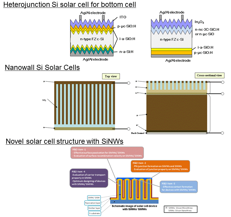
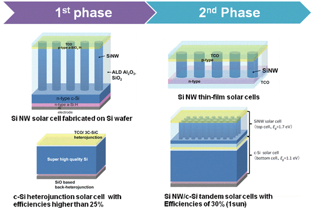
 Nano-Wire Solar Cells
Group3-1 High efficiency Si solar cells

Makoto Konagai
Professor, Advanced Research Laboratories, Tokyo City University- 1. Objectives
- Realization of nano-wire/silicon tandem solar cells
- 2. Methods
-
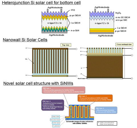
- (1) Develop a new heterojunction solar cells using nanocrystalline 3C-SiC or microcrystalline SiO as hetero-emitter
- (2) We study process technologies to fabricate striped nanowalls with a width of several nm, passivation method for the surface of nanowalls, and electrode formation and interconnection method for output current
- (3) Develop basic technology such as junction-formation, surface-passivation, and contact-formation on silicon microwire structure
- 3. Goal
-
- (1) Make samples of tandem solar cells in which a nano-wire solar cell and Si heterojunction solar cell are stacked in a monolithic or mechanical manner and demonstrate 30% conversion efficiency
- (2) Fabricate test samples by applying state-of-art process technologies developed for ULSI
- (3) Development of basic technology such as junction-formation, surface-passivation, and contact-formation on silicon microwire structure including technology for appropriate evaluation of each item, and application of these technologies for nanowire structure
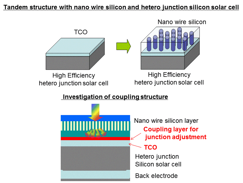
Group3-2 Coupling structure

Kenji Yamamoto
Chief, Photovoltaic & Thin Film Device Research Laboratories. Kaneka Corporation- 1. Objectives
- Investigation of optical and electrical coupling technique between top cell and bottom cell in the high efficiency nanowire silicon/ hetero junction silicon tandem solar cells
- 2. Methods
- Develop techniques to fabricate optical coupling layer consist mainly of transparent conductive oxide layer to develop these coupling structures
- 3. Goal
-
- (1) Development of techniques to decrease optical and electrical loss at the interface of the top nanowire silicon cell and bottom hetero junction silicon cell
- (2) Development of surface treatment method of transparent conductive oxide layer to fabricate nanowire silicon directly from the surface, which will decrease defects on the growth interface of nanowire silicon

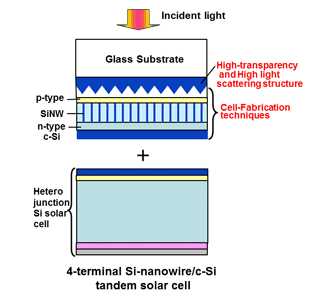
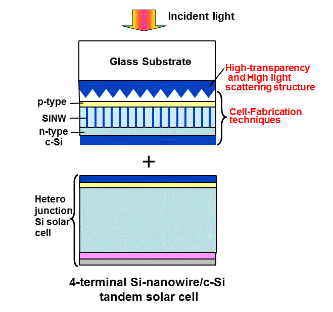
Group3-3 Optical-Confinement and Device-Fabrication techniques

Makoto Tanaka
Device Solution Center, Panasonic Cooperation- 1. Objectives
- Development of Si-nanowire solar cell which has a wide band-gap in order to utilize short-wavelength light more
- 2. Methods
-
- Develop the optical-confinement and the cell-fabrication techniques on Si nanowire solar cell
- 3. Goal
-
- (1) Development of TCO(Transparent Conductive Oxide) material, multi-layer structure and texture shape, which achieve high trasparency and high light scattering in the light incidence side
- (2) Development of p-n junction, passivation and back electrode processes in order to achieve high performance Si-nanowire solar cell