Multilayer ceramic capacitors (MLCCs) (1), which utilize ferroelectric ceramics, are widely used as electronic components in various devices such as smartphones, personal computers, televisions, and automotive systems. With the advancement of mobile devices, home appliances, and IoT technologies, there is an increasing demand for MLCCs to become more compact, offer higher capacitance, and exhibit greater reliability. MLCCs are structured with alternating layers of ferroelectric material and internal electrodes. Within the ferroelectric layers, there are domains with differing polarization directions, as well as domain interfaces on the nanometer (one-billionth of a meter) scale. These domain interfaces are believed to contain charges resulting from changes in polarization, along with compensating charges of opposite polarity that accumulate to maintain electrical neutrality. The state of these charges is considered to influence phenomena such as domain reconfiguration under applied voltage and the generation of leakage current, thereby critically affecting the performance and reliability of MLCCs. However, directly measuring the charge state at ferroelectric domain interfaces (2) at the nanometer scale has remained extremely difficult.
In this study, a research team led by Dr. Takehito Seki, Lecturer at the Institute of Engineering Innovation, School of Engineering, the University of Tokyo, achieved direct measurement of nanometer-scale charge distributions formed at ferroelectric domain interfaces. This was accomplished through the combination of localized charge observation and the observation of atomic displacements on the picometer (one-trillionth of a meter) scale using state-of-the-art electron microscopy. This research marks a significant step toward elucidating the mechanisms of domain interface movement and electrical conductivity in ferroelectric materials. It is expected to lead to a deeper understanding of the intrinsic properties of ferroelectric devices and contribute to future advancements in their performance.
The results of this study were published in the online version of the American scientific journal Science Advances on June 13, 2025.
The results of this development were achieved as part of the research project "SHIBATA Ultra-atomic Resolution Electron Microscopy" supported by the Japan Science and Technology Agency (JST) under the Strategic Basic Research Program ERATO. In this project, JST aims to develop a new measurement technique that can be called an "ultra" atomic resolution electron microscopy that goes beyond conventional atomic resolution electron microscopy, allowing simultaneous observation of atomic-scale structures and electromagnetic field distributions in the temperature range from extremely low to high temperatures. This will enable direct "observation" of the origins of materials and biological functions.
<Notes>
(*1) Multilayer ceramic capacitor (MLCC)
A chip-type ceramic capacitor composed of multiple stacked layers of dielectric materials, such as barium titanate, and electrodes. Taking advantage of the excellent high-frequency characteristics of ceramics, MLCCs achieve both miniaturization and high capacitance, making them widely applicable, such as in electronic devices. The latest smartphones typically contain around 1,000 MLCCs.
(*2) Ferroelectric domain interface
A material that has electrical polarization (spontaneous polarization) even in the absence of an external electric field and whose direction can be reversibly switched by an external electric field is called a ferroelectric material. A region within a ferroelectric body where the polarization is aligned is called a domain, and the boundary between them are known as domain interfaces. Numerous domains and domain interfaces exist within ferroelectric materials, and applying voltage can cause domain interfaces to shift, thereby altering the macroscopic polarization and enabling energy storage.
-
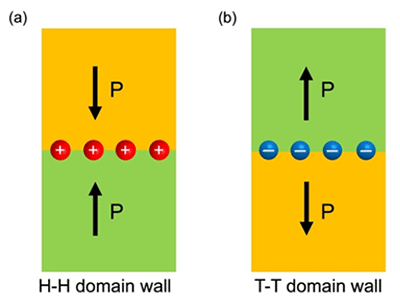
Fig.1 Schematic illustrations of ferroelectric domain walls Schematic illustrations of (a) head-to-head (H-H) and (b) tail-to-tail (T-T) domain walls, respectively. These domain walls carry opposite polarization bound charges at their cores. © Naoya Shibata
-
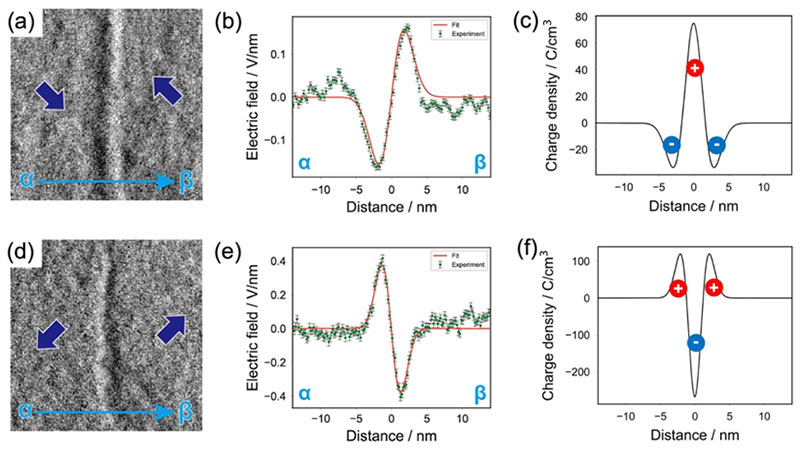
Fig.2 Electric field images of H-H and T-T domain walls in ferroelectric LiTaO3 crystal. (a-c) Horizontal electric field image, electric field line profile, and corresponding charge density profile of the head-to-head domain wall, respectively. (d-f) Horizontal electric field image, electric field line profile, and corresponding charge density profile of the tail-to-tail domain wall, respectively. © Naoya Shibata
Program Information
- JST ERATO
- Research Project “SHIBATA Ultra-atomic Resolution Electron Microscopy”
- JST PRESTO
- Research Area: Precise Molecular Arrangement
- Research Project: Development of Ultra-Low Electron Dose STEM Technique and Structural Analysis of Atomic and Molecular Arrangements in Real Space
Journal Information
Masaya Takamoto, Satoko Toyama, Takehito Seki, Toshihiro Futazuka, Scott D. Findlay, Yuichi Ikuhara, and Naoya Shibata, “Real-space observation of polarization induced charges at nanoscale ferroelectric interfaces”, Science Advances. Published online June 13, 2025, doi: 10.1126/sciadv.adu8021
Contact
-
[About Research]
Satoko Toyama, Assistant Professor,
Institute of Engineering Innovation, School of Engineering, The University of Tokyo
Tel:+81-3-5841-7689
E-mail: toyama sigma.t.u-tokyo.ac.jp
Takehito Seki, Lecturer,
Institute of Engineering Innovation, School of Engineering, The University of Tokyo
Tel:+81-3-5841-7689
E-mail: sekisigma.t.u-tokyo.ac.jpNaoya Shibata, Professor and Director,
Institute of Engineering Innovation, School of Engineering, The University of Tokyo
Tel:+81-3-5841-0415
E-mail: shibatasigma.t.u-tokyo.ac.jp -
[About Program]
Satoko Nagai
Department of Research Project, JST
E-mail: eratowwwjst.go.jp