Kyulux Inc. used materials informatics(1) that combines quantum chemistry calculations and machine learning and succeeded in achieving higher efficiency and longer lifetime for unique OLED technology: Hyperfluorescence™.
In material design, materials informatics was used to select new TADF (Thermally Activated Delayed Fluorescence) materials(2). Compared to the conventional material development method that combines knowledge of researchers and quantum chemistry calculations, promising materials could be discovered 10 times faster. Furthermore, from the perspective of electric charge balance, the emissive layer was optimized and the target lifetime was achieved with colors necessary for full-color display: red, green, and blue. Specifically, four times longer than the target lifetime was achieved for red. Even for blue, of which long lifetime is difficult to achieve, its lifetime could be increased 100 times or longer than at the start of the program.
In the future, based on this result, OLED with a higher resolution, a higher brightness, a better efficiency, and a lower cost is expected to be achieved, and this technology will become widely distributed as the next generation luminescence technology.
<Development content>
- 1. Material development by Materials Informatics
- In the present development, we achieved the goal in a short period of time through materials informatics system (Kyumatic) where machine learning, quantum chemistry calculations, and experiments are integrated. Based on materials proposed by engineers, 10,000 or more candidate materials are prepared by a computer based on the material design rules. For not all the candidate materials, but several hundred, quantum chemistry calculations are performed. The result is used for machine learning by artificial intelligence to predict remaining properties of materials. From the prediction result, promising materials are selected by engineers, and their performances are confirmed by actually synthesizing them. Since experiments are performed after narrowing down the candidates, the development speed is increased by 10 -fold or more. Furthermore, the experimental result also goes through machine learning to improve the accuracy of property predictions.
- 2. Higher efficiency and longer lifetime with a focus on the electric charge balance
- In an emissive layer of OLED, energy generated from recombination of electrons and holes is converted to light. In the emissive layer, host material that transfers electrical energy to luminescent materials generally has high hole-transporting ability; thus, recombination sites for electric charge are concentrated near an electron transport layer. In this development, we increased recombination sites for electric charge by balancing the electron transporting ability and hole transporting ability within the emissive layer to achieve higher efficiency and longer lifetime. By using Co-Host(3) that adds host material with electron transporting ability instead of Single Host(4) that uses one type of host for the emissive layer, we balanced hole transporting ability and electron transporting ability within the emissive layer. In this manner, we expanded the electric charge recombination sites that were biased toward the electron transporting layer throughout the emissive layer. As a result, the ratio of external light emission relative to the injected electrical energy (external quantum efficiency) was improved by 20 to 40%, successfully increasing the lifetime by the maximum of 10-fold.
This development was performed as a company-led phase NexTEP-B type development topic “OLED materials that achieve higher efficiency and purer colors”. NexTEP-B is a technology transfer support program: Adaptable and Seamless Technology Transfer Program through Target-driven R&D (A-STEP) that aims to return research outputs of universities and public research institutions as practical technologies that are important for the national economy to the society. It was commissioned by JST to Kyulux Inc. based on the result of professor Chihaya Adachi and others at Center for Organic Photonics and Electronics Research, Kyushu University, and has been commercially developed.
(1) Materials Informatics
The collective term for a method to search for materials using material database in which material properties are calculated on a computer at a high precision, and artificial intelligence. Compared to the past material search method that depends on researchers’ experiences and intuition, time and cost can be reduced largely.
(2) Thermally Activated Delayed Fluorescence (TADF) material
By reducing the difference in the energy level of singlet and triplet excited states of organic materials, energy of triplet is transferred to singlet, and luminescence with 100% internal quantum efficiency is achieved. It does not require rare metal, and material cost can be reduced. Generally, it has wide emission spectrum, and purity of the colors is too low for applying displays.
(3) Co-Host
The emissive layer of OLED is prepared by doping emissive material to a host material. This method uses two types of host materials. It is used to improve performance of OLED.
(4) Single Host
A method that uses one type of host material for the emissive layer.
-
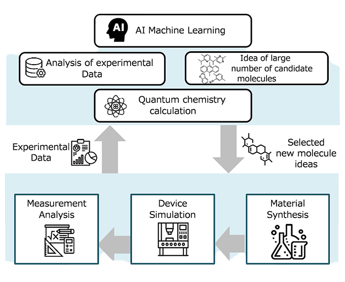
Fig.1., Kyulux's materials informatics "Kyumatic" Kyumatic is composed of functions such as machine learning, quantum chemistry calculation, generation of a large number of candidate molecules, and analysis of experimental data. Kyumatic can be used to suggest new molecular ideas. The evaluation results such as the physical properties of the synthesized material are feedback to the system in order to improve the prediction accuracy of the material properties. In the future, Kyulux plans to feedback the evaluation results of devices using new materials and expand the scope of application not only to material search but also to device optimization.
-
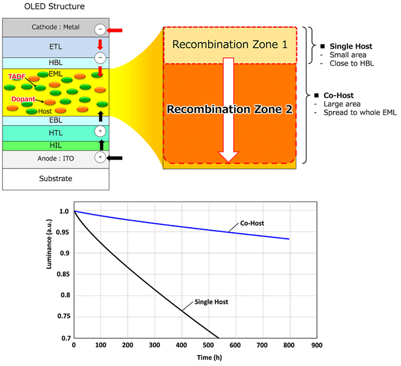
Fig.2., High efficiency and long lifetime of OLED focusing on charge balance The Co-host expanded the recombination zone, which was previously biased toward the electron transport layer to the entire light-emitting layer, and the compounding ratio of the host was optimized. As a result, the time until the brightness decreased by 5% was 10 times or more, and the lifetime was extended.
Program Information
- JST A-STEP (Adaptable and Seamless Technology Transfer Program through Target-driven R&D)
- NexTEP-B type
- Development Theme: high efficiency and high purity color development OLED light emitting material
Contact
-
[About Research]
Yabuta Akira
R&D Planning Office,
Kyulux Inc.
E-mail: info kyulux.com
 -
[About Program]
Okishiro Miho
Department of Business Innovation Development, JST
E-mail: jitsuyokajst.go.jp