Progress Report
Development of scalable Silicon quantum computer technology[1] Development of scalable fault-tolerant Si qubit devices
Progress until FY2024
1. Outline of the project
This research project aims to develop scalable silicon (Si) qubit technologies suitable for fault-tolerant quantum computing. Our focus is to develop high-fidelity qubit control, demonstrated in small-scale systems, in a scalable architecture considering qubit layout, device fabrication process, and control signal integrity for fault tolerance. We pursue the realization of truly scalable Si qubit devices by establishing these core technologies.

In this project, we fabricate Si/SiGe quantum well qubit devices, which offer excellent uniformity across the sample and enable electrical control of qubit parameters (Figure 1). With the help of the industrial manufacturing processes, we aim to provide a blueprint for large-scale fault-tolerant quantum computing.
2. Outcome so far
- Preparation of a 12-qubit device and an experimental setup
- Demonstration of single-qubit gate fidelity exceeding 99.99%
- Analysis of error mechanisms in two-qubit controlled-phase gate and development of calibration methods
- Demonstration of fast, high-fidelity qubit readout and active reset via feedback, essential for quantum error correction
- Development of pulse signal generators and through-silicon via (TSV) processes for signal transmission suitable for large-scale qubit control
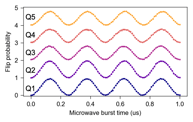
We analyzed single- and two-qubit gate errors via gate set tomography and randomized benchmarking. By optimizing control pulse envelopes, we achieved control fidelities competing with the highest reported values so far (Achievements 2 and 3). In addition, we detected and analyzed noise correlations between qubits that help to understand error mechanisms in spin qubits.
We also demonstrated high-speed (in 1 microsec) and high-fidelity (>99%) qubit readout and bit-flip/reset operations via feedback control—key components of quantum error correction (Achievement 4).
We also developed a pulse signal generator for the precise control of a large number of qubits. To compensate for the degradation of pulse waveforms inside a dilution refrigerator, we implemented an innovative calibration circuit capable of high-resolution waveform shaping and verified its performance through experimental evaluation (Fig. 3(a)). Furthermore, to ensure signal integrity for signal transmission to densely integrated qubits, we developed a through-silicon via (TSV) formation process on a silicon interposer, which enables a wire-bond-free chip packaging structure (Fig. 3(b), Achievement 5).

All these efforts lead to the development of the new 12-qubit devices and experimental setups for conducting high-fidelity 12-qubit experiments (Achievement 1).
3. Future plans
We have clarified the technical requirements for high-fidelity qubit control and advanced our understanding of error mechanisms. These results will allow us to address emerging challenges in integrated qubit devices, such as distant qubit coupling via spin shuttling and signal integrity with high-density wiring. We then aim to design scalable Si qubit devices optimized for fault-tolerant operation and advance our research toward large-scale quantum computing.