Research Results
Deployment of Spintronics Low-Power Semiconductor Technology
Toward Mass Production of the Low Power Consuming and High-Speed Operating Vertical Body Channel-MOSFETFY2025
- ENDOH Tetsuo (Director, Center for Innovative Integrated Electronic Systems, Tohoku University)
- CREST
- Research Director (2008-2013), Research of Innovative Material and Process for Creation of Next-generation Electronics Devices Area: Research and Development of Vertical Body Channel MOSFET and Its Integration Process
- ACCEL
- Research Director (2014-2018), Three-Dimensional Integrated Circuits Technology Based on Vertical BC-MOSFETs and Its Advanced Application Exploration
Realization of dramatically low power consumption and high-speed operation with vertical body channel transistor and MRAM
A research group led by Director Tetsuo Endoh of the Center for Innovative Integrated Electronic Systems, Tohoku University has developed the world's first low power consuming and low noise innovative transistor, vertical body channel (BC) MOSFET*1, which serves as the source of the GAA-type MOSFET that is now being actively developed in the 3 nm and later CMOS generations. The research group has built a prototype of a 1-gigabit (giga: 1 billion) class large-scale dynamic random-access memory (DRAM)*2 in which the vertical BC-MOSFET is placed in the peripheral circuits of memory cells, using wafers with a large diameter of 300 mm. The DRAM has been shown to operate well even under voltage conditions that are significantly lower than conventional DRAMs. This vertical BC-MOSFET (vertical GAA-MOSFET) is also listed as a standard technology for 3 nm and beyond in the International Roadmap for Devices and Systems (IRDS) on semiconductor technologies.
Further, the research group has also been working on base technologies to apply the vertical BC-MOSFET to magnetoresistive random access memory (MRAM), a spintronics semiconductor, and has successfully demonstrated the world's highest performing write speed with a 128-megabit (mega: 1 million) spin-transfer torque MRAM (STT-MRAM)*3 prototype.
For implementation to society of these results, the Tohoku University startup company, Power Spin Inc., was established in 2018. Director Endoh, who also serves as Representative Director & COO of Power Spin Inc., is advancing research and development for the practical application and mass production of STT-MRAM and other spintronics low-power semiconductors*4 through collaboration with semiconductor manufacturers. In 2018, mass production of MRAM has begun from Taiwan's global semiconductor foundry, Taiwan Semiconductor Manufacturing Company Limited (TSMC), and others.
*1 MOSFET
A metal-oxide-semiconductor, field effect transistor. The most common structure in integrated circuits.
*2 DRAM
Dynamic random-access memory. A recording device that reads and writes information.
*3 STT-MRAM
Spin-transfer torque magnetoresistive random access memory. Non-volatile memory that stores information in the direction of magnetization. Its high-speed magnetization reversal enables high-speed operation, and the absence of atomic migration allows high rewrite resistance.
*4 Spintronics low-power semiconductor
Spintronics is a compound term from spin and electronics. While conventional semiconductors handle the presence or absence of electric charge as "0" or "1" information, spintronics semiconductors use the difference in the magnetic orientation (electron spin) generated by the rotation of electrons to handle information. Although conventional semiconductors lose information when the power is turned off, magnetic force is not lost when the power is turned off, thereby potentially allowing significant reduction in power consumption.
Reduction in standby power and leaked power as the key to low power consumption
Due to the increasingly high functionality of smartphones and tablet devices, shortening battery life has become a major issue.
One factor is the standby power of semiconductor devices. Current central processing units (CPU) and DRAMs lose data when the power is turned off and therefore require standby power that can be energized even when they are not operating. Spintronics semiconductors are being developed as a means to resolve this problem. Spintronics semiconductors record information based on the magnetic orientation prompted by the electron spin (rotation). Magnetic force is stored even when the power is turned off and therefore does not require standby power, allowing for a reduction in power consumption to approximately one-hundredth in theory. Tohoku University is the world's leading institution in spintronics semiconductor research, and MRAM is already being mass-produced by semiconductor manufacturers worldwide.
Another factor is the leaked current in the MOSFET itself, the basic element in integrated circuits. A semiconductor device (transistor) transfers information in and out by passing and blocking currents at the gate. As devices continue to miniaturize to the nano-size, the gate length also shortens. This has caused external current leaking that is not negligible and affected power consumption (Fig. 1). To resolve this problem, Director Endoh and colleagues have been researching the vertical BC transistor. This vertical BC-MOSFET (vertical GAA-MOSFET) is also listed as a standard technology for 3 nm and beyond in the IRDS on semiconductor technologies.
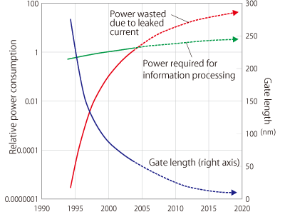
Fig.1 Leaked Current in Semiconductor Integrated Circuits
In semiconductor integrated circuits, leaked power is rapidly increasing as gate lengths shorten.
(Created based on IEEE Computer,36(12):68-75,2003 [dotted lines represent projections at the time])
Engaging in the development of devices using the vertical body channel-MOSFET under industry-academia collaboration
The research group led by Director Endoh has been conducting basic research on vertical BC transistors. While conventional transistors form a flat circuit on the silicon substrate, the vertical BC transistor comprises a structure in which the gate is wrapped 360 degrees around a silicon cylinder of several tens of nanometers in diameter. This allows for sufficient gate length and thus significantly reduces leaked current (Fig. 2). However, it was difficult to form insulating films on ultra-thin silicon cylinders. During five years of research, the research group identified that the formation of insulating films was inhibited by the change in the degree of oxidation due to the direction (plane orientation) of silicon crystals and developed the world's first 1-megabit vertical BC memory (Fig. 3).
Based on these results, since 2014, the research group has been advancing research and development to develop novel devices that enable ultra-low power consumption and high-speed operation by combining the vertical BC transistor technology with spintronics semiconductor technology. The project involved not only universities but also leading semiconductor-related companies such as Tokyo Electron Ltd. and Micron Japan Ltd., and has been developing base technologies to realize dramatically higher integration and low-power properties of the vertical BC-MOSFET and common base technologies that will lead to applications, including primarily working memory (e.g., DRAM, STT-MRAM) as well as logic large-scale integration (LSI), analog LSI, and AI or brain-type LSI*5.
Through this research, the research group built a prototype of a gigabit-class, large-scale STT-MRAM with the vertical BC-MOSFET placed in the peripheral circuits, successfully demonstrated operability at low power supply voltage for the first time in the world, and established an integration process technology to realize high-density, high-speed MRAM. The research group also succeeded in significantly reducing the area and standby power of SRAM in logic LSI.
In parallel with such research and development, the Tohoku University startup company, Power Spin Inc., was established in 2018, and research and development for the practical application of the vertical BC-MOSFET, on aspects including manufacturing cost, durability, and reliability, is underway through industry-academia collaboration centered around the Center for Innovative Integrated Electronic Systems.
*5 AI and brain-type LSI
AI semiconductors that utilize neuromorphic technology which replicates the structure of the brain.
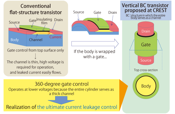
Fig.2 Structure of the Vertical Body Channel Transistor Transistors transmit signals by creating electrical paths (channel) with gate voltage and allowing electricity to flow from the source to the drain. When the gate length is shortened, leaked currents pass through even when no channel is created due to the voltage between the source and drain. The aim of the vertical structure is to reduce the voltage between source and drain, which causes the leakage.
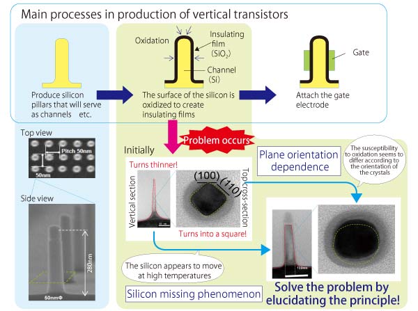
Fig.3 Main Process in the Production of Vertical Transistors The "missing phenomenon" (center), or the thinning of silicon cylinders, which was first revealed by creating nano-level crystals, and the "plane orientation dependence" (bottom right), which led to the solution of the problem.
Participation in the development of photonics-electronics convergence semiconductors that contribute to the realization of ultra-fast AI
Leveraging the results of this research, Power Spin jointly developed a contactless, multi-person temperature screening camera with IRIS OHYAMA Inc. While conventional temperature screening cameras can screen 5-10 persons/second, this camera can screen at a high speed of 40-170 persons/second. The device was demonstrated at the May 2023 Hiroshima G7 Summit (Group of Seven) held in the midst of the COVID-19 pandemic.
Further, the Center for Innovative Integrated Electronic Systems, Tohoku University is also participating in a project on photonics-electronics convergence semiconductors, in which NTT and others under international collaboration are developing the semiconductor as a core technology for next-generation Innovative Optical and Wireless Network (IOWN), undertaking parts of development activities for memory controller technologies. As such, the center continues research and development activities to contribute to the development of future devices that require ultra-high speed.