Research Results
Starting Point for Atomic Scale Manufacturing
Realization of Mass Growth of Metallic Nanowire and Elucidation of its PrincipleFY2025

- KIMURA Yasuhiro (Associate Professor, Faculty of Engineering, Kyushu University)
- PRESTO
- Researcher (2020-2024), Nanomechanics Area: Crystalline Design of a Metallic Nanowire Based on Electromigration
Development of method for mass growth of forest-like aluminum nanowires
A research group led by Associate Professor Yasuhiro Kimura at Faculty of Engineering, Kyushu University, used the atomic diffusion*1 phenomenon that transports atoms in solid matter to develop a method for mass growth of forest-like aluminum nanowires*2.
The linear pure-metal nanowire, also called whisker, is a material with a diameter of one-thousandth thickness of a human hair and a length of several hundred micrometers and is considered one of the most promising materials in nanotechnology. In particular, the single-crystal pure-metal nanowire that independently grows on solid substrates is garnering attention as a broad-use constituent material for micro and nano devices, including its application in gas sensors and biomarkers as next-generation sensing devices and plasmonic waveguides*3 as next-generation optoelectronics.
However, unlike semiconductor nanowires, carbon nanotubes composed of organic materials, and metallic oxide nanowires, for which mass synthesis methods have already been established, technologies to mass produce single-crystal pure-metal nanowires had not been established.
The present research successfully developed a technology to grow aluminum nanowires by using the simple method of ion beam irradiation to control the distribution of crystal grains*4 in metallic thin films and applying specific stress*5 for atomic transport in order to collect a large number of metal atoms to a targeted location (Fig. 1).
This result paves the way for the practical application of the bottom-up method of pure-metal nanowire growth, which had been able to produce only small amount accidentally. This may serve as a starting point for technologies in atomic-scale manufacturing of metals.
*1 Atomic diffusion phenomenon
An atomic transport phenomenon in solid matter that is driven by atomic concentration gradients, hydrostatic stress gradients, temperature gradients, and electric potential gradients.
*2 Nanowire
A linear nanostructure with a diameter of about one-thousandth thickness of a human hair (approximately 100 to 600 nanometers).
*3 Plasmonic waveguide
On metal surfaces, light exists in a state that is bound to metallic electrons (surface plasmon polariton). A waveguide that leverages this property is called a plasmon (plasmonic) waveguide, which can guide light in a state confined in a nanometer-level area.
*4 Crystal grain
A solid mass in which atoms are regularly arranged. The present research uses ultrafine grains ranging from several nanometers to several tens of nanometers.
*5 Stress
Force per unit area against a virtual surface that acts inside matter.
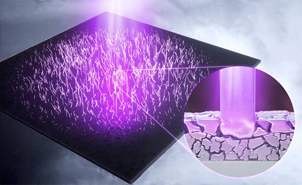
Fig.1 Aluminum nanowires grown like a forest on metallic thin films
Aluminum nanowire as a promising nanocomponent
In recent years, pure-metal nanowires have demonstrated not only high strength due to their monocrystal and low-defect properties, but also anomalous scattering of electrons and phonons in electrical and thermal conductivity, and surface light propagation and emission arising from plasmonic phenomena.
In particular, vertically self-grown aluminum nanowires have an immense surface area, demonstrate the ability to semi-permanently maintain favorable electrical properties due to their resistance to natural oxidation, and exhibit exceptional mechanical properties including strength, hardness, and extensibility owing to their monocrystals. Given these unique characteristics, the potential use of the material as a promising nanocomponent in sensing devices and optoelectronics is attracting attention.
For this application, the development of methods for stable mass production of aluminum nanowires is indispensable. For carbon nanotubes and semiconductor nanowires, mass synthesis methods that supply raw materials in gas form and facilitate growth using reactions with catalysts on substrates have been established. However, aluminum is hard to supply in gas form due to its low vapor pressure, and even if it could be supplied, catalysts serving as the core of growth have not been identified, rendering current methods inapplicable. Therefore, the establishment of an original nanowire growth method was in urgent need.
Employment of atomic diffusion and establishment of a mass growth technology
The difficulty in growing metallic nanowires lies in the mechanism of the growth. Since they grow from the root alike trees, metal atoms for nanowire growth in the solid matter serving as base material needs to be transported in large quantity to the targeted location. However, unlike in gases or liquids, atoms in solid matter are less active and difficult to transport.
The research group employed atomic diffusion, a nano-scale substance transport phenomenon, as a means of transporting atoms in large volume in solid matter and established a technology that grows large amounts of aluminum nanowires at targeted locations alike forestation. The key to this achievement is the production of driving force, which is the source of atomic diffusion, through the focus on crystal grains inside thin films. The research group used ion beam irradiation to coarsen the grains only in the surface layer of thin films and created a grain gradient with coarse grains on the thin film surface layer and fine grains on the thin film lower layer. The mechanism of the grain gradient triggering an increase in the driving force of atomic diffusion was revealed through electron microscopic observation and numerical calculation based on finite element analysis*6.
When a thin film is heated following ion beam irradiation, the atoms are transported in several sequences described below, facilitating the preparation for nanowire growth. First, when the thin film is heated, the grain size dependence of yield stress*7 causes the grain gradient to prompt an upward flow of the atoms, and many atoms are transported to the thin film surface. Subsequently, the orientation dependence of yield stress causes the atoms to flow toward specific grains. This series of atomic flow is based on hydrostatic stress*8 gradient, and its value can be calculated using finite element analysis. Grains that have stored a large volume of atoms in such ways grow as nanowires in a vertical direction, as if to release the atoms (Fig. 2 and 3).
*6 Finite element analysis
One of the analytical methods for clarifying continuum mechanics problems.
*7 Yield stress
The critical stress value at which a material deformed by load application does not return to its original state even if the load is removed (i.e., the deformation effects remain). It is an indicator of material strength.
*8 Hydrostatic stress
Stress acting vertically on the surface of a matter, such as the pressure exerted on an object submerged in water. Also called mean normal stress.
*9 STEM-EBSD
STEM: Scanning transmission electron microscopy. A microscopy that irradiates and scans a narrowly focused electron beam onto a sample and detects and creates images of transmitted or diffracted waves emitted from the irradiated point. Small matter can be observed more so than scanning electron microscopy (SEM).
EBSD: Electron backscattered diffraction. A method to analyze the orientation indicating the degree of crystal grain inclination.

Fig.2 A cross-section STEM-EBSD*9 image of a thin film with a nanowire (top). Sequence of wire growth (bottom).
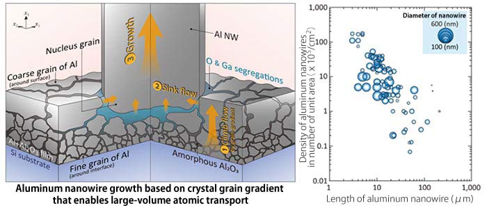
Fig.3
An image showing the growth mechanism of an aluminum nanowire (left). A thin film comprising aluminum and aluminum oxide deposited on a silicon substrate. (1) Atoms flow upward. (2) Atoms flow in. (3) An aluminum nanowire grows.
A graph of the density (in number of units) and length of nanowires grown in the experiment (right). The maximum vertical axis value was 180 × 105 units per cm2.
Elucidation of the principle of the growth process
The results not only realized mass growth of metallic nanowires but also clarified the mechanism of the growth process by using a combination of transmission electron microscopy observations and numerical simulation based on finite element analysis.
This growth process is not limited to aluminum and can be extended to other metals in principle. It may therefore be the starting point for metallic nanowire production technologies based on atomic self-assembly, which has been untapped so far. Of note, the maximum density of aluminum nanowires produced by atomic diffusion was 2 × 10⁵ units per cm2 (surface coverage of 0.04%) reported in 1975. The present research demonstrated after half a century that a larger maximum of 180 × 105 units per cm2 could be obtained.
This research may lead to the generation of atomic-scale manufacturing technologies oriented toward application to micro and nano devices.