Research Results
A Small, Highly Efficient, Low-cost Light Source that Dramatically Enhances Semiconductor Laser Brightness
Achievement of High-Brightness Enhancement of Photonic Crystal LasersFY2024
- NODA Susumu (Professor, Graduate School of Engineering, Kyoto University)
- ACCEL
- Research Director (2013-2017), “Photonic Crystal Surface-Emitting Semiconductor Laser- Towards Realization of High Power and High Brightness Operation”
World-first achievement of brightness of 1 GW cm-2 sr-1, equivalent to that of large-scale lasers
Semiconductor lasers are small, highly efficient, low-cost light sources. The research group led by Susumu Noda, professor of the Graduate School of Engineering, Kyoto University, has succeeded in enhancing the brightness*1 of a semiconductor laser to 1 GW cm-2 sr-1 based on “Photonic crystal surface-emitting laser (PCSEL)”*2 technology. This brightness is equivalent to that of existing large-scale lasers, such as CO2 lasers, solid-state lasers, and fiber lasers.
PCSEL technology makes it possible to cut or process objects such as metals using only semiconductor lasers. This achievement dramatically expands the application range of semiconductor lasers. In particular, it is expected to revolutionize the field of smart manufacturing, where digitization of manufacturing processes is underway.
One of the most important issues of conventional semiconductor lasers is that they cannot be directly used for laser processing. This is because their beam qualities deteriorate when the sizes of semiconductor lasers are expanded to obtain a high output power, making high brightness unachievable. To resolve this issue, the research group has been conducting research on PCSELs that incorporates a two-dimensional photonic crystal inside the semiconductor laser. Recently, the group was the first in the world to successfully realize operation with output powers of 50-100 W and a brightness of 1 GW cm-2 sr-1. This was achieved by using a PCSEL with a diameter of 3 mm and precisely controlling optical couplings inside the device. In addition, the group has also developed design guidelines that enable single-mode operation without compromising beam quality even when the device size is enlarged to a diameter of 10 mm, indicating that even an output power of 1 kW with a brightness of 10 GW cm-2 sr-1 is achievable. These results indicate that PCSELs will completely replace large-scale lasers in the future, thereby bringing about the aforementioned revolution.
*1 Brightness
An indicator of how strongly laser light can be focused or how narrowly the beam spreads out. Brightness can be defined as the light output per unit area or per unit solid angle. Realization of high-brightness operation of the laser is extremely important for laser processing and advanced sensing. Brightness has a close relationship with beam quality: the higher the beam quality, the higher the achievable brightness.
*2 Photonic crystal surface-emitting laser
A photonic crystal is a material that has a periodic refractive index distribution on the order of the wavelength of light. Such crystals are attracting attention as photonic nanostructures that enable various types of photonic control. A semiconductor laser incorporating two-dimensional photonic crystals (photonic nanostructures with a periodic refractive index distribution on the order of the wavelength of light arranged periodically in two dimensions) and operating at singularity
( , etc.) points of their band structure is called a photonic-crystal surface-emitting laser (PCSEL). Such lasers are capable of forming stable standing wave states over large areas, resulting in the emission of high-power, high-quality beams.
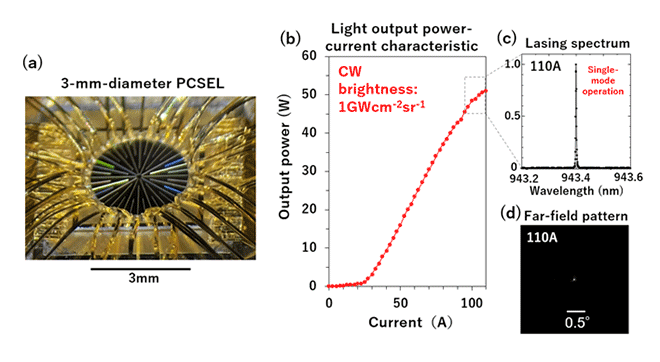
Fig. 1 Photo (a) and laser characteristics (b) of the developed PCSEL
Continuous wave operation with a high beam quality was successfully achieved with a light output power of over 50 W in a single mode, with an extremely narrow beam divergence angle of 0.05°. The achieved brightness reached 1 GW cm-2 sr-1, which is equivalent to those of bulky lasers such as CO2 lasers, solid-state lasers, and fiber lasers.
Research on PCSELs that began in 1999 has come to fruition
The PCSEL was invented in 1999 by Professor Noda at Kyoto University. Since then, research and development have been carried out to achieve higher output power and higher brightness for PCSELs.
The fundamental reason why it has not been possible to increase the brightness of conventional semiconductor lasers is the deterioration of beam quality caused by the higher-order modes, which are generated when the device size is enlarged to increase the light output power, having multiple antinodes in their resonant mode profiles (electromagnetic field distributions).
The PCSEL invented by Professor Noda is based on the large-area resonance effect at a singularity point of the two-dimensional photonic crystal, which enables operation in a fundamental mode to be maintained over a large area. In 2014, it was demonstrated that no higher-order modes appeared even when the device size was expanded to a diameter of 200 µm, which led to the realization of Watt-class high-output single-mode operation. When the device size was expanded further to increase the output power, however, higher-order modes started to appear, making it difficult to enhance the brightness. To overcome this issue, the research group invented a new photonic crystal structure, a so-called “double-lattice photonic crystal”*3. Based on this structure, they established a way to suppress the occurrence of higher-order modes even when the photonic crystal laser area is significantly expanded (≥3mm), enabling the brightness to be enhanced much more than before.
The basic concept is to selectively increase the losses of the higher-order modes while keeping the loss of the fundamental mode low (see Fig. 2), thereby preventing beam quality deterioration. As shown in Fig. 2 (b), the in-plane light diffraction is weakened by adjustment of the distance of elliptical and circular lattice points in the double-lattice structure and fine balancing of the sizes of these lattice points. In addition, the in-place light diffraction effect is further weakened though fine adjustment of the in-plane light diffraction via radiative waves, which form the emitted laser beam. As a result, the emission angle dependence of radiation loss becomes steep, as shown in the theoretical calculations in Fig. 2 (d), where it should be noted that the fundamental mode is emitted in the vertical direction while the higher-order modes are emitted in oblique directions (see Fig. 2 (c)). It is seen in Fig. 2(d) that only the radiation losses of the higher order modes emitted in oblique directions can be increased while maintaining low radiation loss of the fundamental mode emitted in the vertical direction. This indicates that it is possible to prevent the occurrence of higher-order modes and to increase the brightness.
*3 Double-lattice photonic crystal
A new photonic crystal in which a pair of two-dimensional photonic crystals are overlapped with a shift of approximately one-quarter wavelength in the x and y directions. Typically, one of the photonic crystals has an elliptical lattice-point structure, while the other photonic crystal has a circular lattice-point structure.
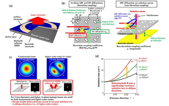
Fig.2 Adjustment of the double-lattice structure of the photonic crystal laser
(a) Schematic diagram of the structure of a PCSEL with a double-lattice photonic crystal.
(b) Schematic diagram of the diffraction effects (mutual couplings) of light waves in a double-lattice photonic crystal. In addition to coupling due to diffraction at angles of 180° and 90° within the plane of the photonic crystal (called Hermitian coupling due to the absence of radiation loss, and whose sums of their coupling coefficients' real and imaginary parts are denoted as R and I, respectively), shown in the left panel, coupling accompanying diffraction at angles of 180° via radiative waves (called non-Hermitian coupling due to the presence of radiation loss, and whose magnitude is denoted as µ), shown in the right panel, is taken into account. The total effect of diffraction is thus reduced.
(c) Light intensity distributions in the fundamental mode and a higher-order mode of 1st order (top) and schematic diagrams of their emitted beams (bottom).
(d) Calculated dependence of radiation loss on radiation angle for structures with different values of R and µ. The value of I was adjusted to obtain an appropriate radiation loss (approximately 10 cm-1) in the vertical direction (= fundamental mode) for each structure.
A device with a 3-mm diameter that enables single mode operation in the range of 50 to 100 W
Based on the strategy shown in Fig. 2, single-mode operation in the range of 50 W to 100W with a brightness of 1 GW cm-2 sr-1 is expected with a PCSEL having a 3-mm diameter. The research group fabricated a PCSEL with a 3-mm diameter (see Fig. 3(a)), conducted detailed measurement of its photonic band structure and radiation characteristics, and experimentally evaluated its coupling coefficients. This evaluation confirmed that the desired coupling coefficients were achieved.
The lasing characteristics of the device were then evaluated under a pulsed and low current injection condition so that a thermal effect does not occur. From the current-light output power characteristics shown in Fig. 3 (b), it is clear that the laser oscillation was obtained with a threshold current of 20 A. The far-field pattern and its intensity profile during laser oscillation (Fig. 3 (c), (d)) show that the oscillation was achieved with an extremely narrow beam divergence angle (of as low as 0.05°), indicating that the lasing oscillation occurred only in the fundamental mode over the 3-mm-diameter area. This is due to the aforementioned appropriate reduction of the total effect of light diffraction (i.e., simultaneous reduction of the coupling coefficients R and µ shown in Fig. 2 (d)).
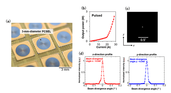
Fig. 3 The fabricated photonic crystal laser with a 3-mm diameter and its evaluation
(a) Photograph of the developed photonic crystal laser with a 3-mm diameter.
(b) Light-output characteristics under pulsed conditions at a low injection current.
(c) Far-field pattern.
(d) Intensity profile. High-beam-quality operation with an extremely narrow beam divergence angle (up to 0.05°) was achieved.
As described above, high-beam-quality operation in the fundamental mode was demonstrated under pulsed conditions. However, for laser processing, it is necessary to achieve high-beam-quality operation even under continous-wave conditions at a high injection current. In this case, the device temperature increases due to Joule heating, and a temperature distribution is generated inside the device (Fig. 4 (a)). Such thermal effects disturb the optical couplings inside the device, making high-beam-quality operation difficult. Therefore, the research group introduced a pre-installed lattice constant distribution as shown in Fig. 4 (b), so that these thermal effects can be cancelled and the optical couplings inside the device can be maintained during continuous-wave operation. By doing so, the realization of single-mode, high-beam-quality operation is expected.
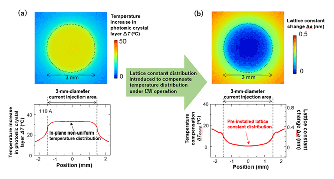
Fig. 4 Introduction of a lattice constant distribution that compensates for the effect of temperature changes caused by continuous operation at a high injection current
(a) The temperature distribution in the plane of the device and its cross-sectional profile during continuous operation (with 110-A injection current) of a photonic crystal laser with a 3-mm diameter.
(b) The lattice constant distribution introduced to cancel out the in-plane temperature distribution during continuous operation.
Fig. 1 (a) above shows a PCSEL with a 3-mm diameter, incorporating both a mechanism to appropriately reduce the total effect of diffraction (simultaneously reducing the coupling coefficients R and µ) and a mechanism to maintain the reduced effect of diffraction throughout the device area during continuous operation. As shown in Fig. 1 (b), a maximum light output power exceeding 50 W was achieved while realizing single-mode operation in the fundamental mode, as shown in Figs. 1 (c) and (d), thereby enabling high-beam-quality operation with an extremely narrow beam divergence angle (of as low as 0.05°). Through these development processes, a brightness of 1 GW cm-2 sr-1 was achieved with a photonic crystal surface-emitting laser. This brightness is equivalent to that of large-scale lasers and is at the level required for laser processing.
Potential of expanding the device area to completely replace existing large-scale lasers
By arraying the newly developed PCSELs in two dimensions, it becomes possible to increase the light output power to the level of kilowatts and beyond while maintaining the same brightness. Moreover, as described above, the research group has already designed a device with a 10-mm diameter that is capable of complete single-mode operation with kW-level light output power and a brightness of over 10 GW cm-2 sr-1. The group is planning to realize such kW-level high-brightness PCSELs and even to make arrays of such high-brightness PCSELs. When such devices are realized, it is expected that they will replace existing large-scale lasers, as shown in Fig. 5, thereby revolutionizing the field of smart manufacturing. In addition, the potential applications extend not only to laser processing but also to new fields such as space applications (propulsion light sources for solar sails), laser fusion, and excitation sources for EUV exposure equipment.
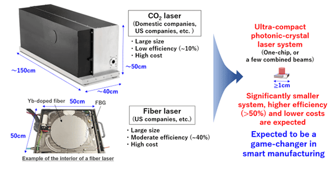
Fig. 5 Comparison of large-scale lasers and a photonic-crystal surface-emitting laser
