Research Results
Creating next-generation memory with ultrahigh-speed and minimal power consumption
World-leading study of topological antiferromagnetsFY2023

- NAKATSUJI Satoru (Director, Trans-scale Quantum Science Institute, the University of Tokyo)
- CREST
- Research Director(2018-2024)of the project "Functional Magnets and Devices based on Topological Electronic Structure" in the research area of "Creation of Core Technology based on Topological Materials Science for Innovative Devices"
- JST-Mirai Program
- Program Manager(2020-2030)"Innovation of Photoelectric Technologies using Spintronics" (Large-scale Type)
Development of information writing and current control technologies for antiferromagnetic memory devices
The research team is engaged in studying a topological antiferromagnetic metal*1, Mn3Sn (Fig. 1), to develop nonvolatile memories that may lead to next-generation terahertz electronic devices. Moreover, through the research on Mn3Sn, the team has succeeded for the first time in realizing "quantum tunneling magnetoresistance that does not require magnetization", defying common sense of nonvolatile magnetoresistive random access memory (MRAM). This finding builds a solid foundation for future high-speed, low-power information processing technology exceeding the performance of contemporary silicon semiconductor technology.
(1) Demonstration of ultrafast spin dynamics in topological antiferromagnetic metals
Using the topological antiferromagnetic metal Mn3Sn, the research team detected real-time spin dynamics and demonstrated that the switching speed is faster than 10 picoseconds (1 picosecond is a trillionth of a second). This corresponds to a reading/writing speed 10 to 100 times faster than that of the current commercialized MRAM, indicating that the topological antiferromagnet has exceptional potential for building ultrafast MRAM.
(2) Piezomagnetic effect*2 allows information writing in antiferromagnet memory devices
The research team discovered a pronounced piezomagnetic effect at room temperature in the antiferromagnet Mn3Sn, famous for its large anomalous Hall effect*3 despite nearly absent magnetization. This is the first-ever demonstration that the sign of the anomalous Hall effect, usually controlled by an applied magnetic field, can be effectively controlled by strain. This observation defies conventional wisdom since the initial discovery of the anomalous Hall effect in 1880. This study also showed that the anomalous Hall effect originates from the cluster magnetic octupole, not magnetization.
(3) World's first current control of the perpendicular binary states in antiferromagnets
Spintronic applications have seen significant advances by turning to antiferromagnets because antiferromagnets are insensitive to stray fields and can operate hundreds of times faster than their ferromagnetic counterparts. A major obstacle, though, is the difficulty in controlling the antiferromagnetic spin configuration, which limits the device’s performance. This research team achieved full perpendicular electrical switching of the antiferromagnetic Mn3Sn for the first time, enabled by applied tensile strain. Such switching maximizes the device’s operating speed and dramatically simplifies the device configuration, setting down a vital milestone in antiferromagnetic spintronics.
(4) Discovery of quantum tunneling magnetoresistance at room temperature
Magnetoresistive random access memory (MRAM) can revolutionize computer memory by offering ultrafast, high-density, and energy-saving data storage and processing. A critical step to realizing such a possibility is to improve MRAM's operation speed and integration density; both factors are currently limited by the ferromagnetic materials used for this technology. Antiferromagnets have recently been recognized as key elements for future ultrahigh-speed on-chip MRAM. A critical next step for their applications is demonstrating the quantum tunneling magnetoresistance*4 in all-antiferromagnetic MRAM, which may serve as a reading protocol.
The research team’s new study is the first observation of a room-temperature quantum tunneling magnetoresistance in an all-antiferromagnetic spintronics device with nearly zero magnetization, which was previously thought impossible. This discovery is a significant step toward realizing ultrafast, high-density, low-power MRAM.
*1 Antiferromagnetic metals and ferromagnetic metals
Topological materials cannot be classified as metals, insulators, or semiconductors. A typical example is a topological insulator: its interior behaves like an insulator that does not allow current to flow through, but its surface hosts unique metallic states, enabling fast motion of electrons and is robust against impurities. Each atom in a material carries a spin and acts like a tiny magnet. In antiferromagnets, the spins form antiparallel arrangements and cancel one another, and thus the net magnetization becomes nearly zero. The spins are aligned in one direction in ferromagnets, leading to sizable magnetization. The topological antiferromagnet Mn3Sn is the first example of a magnetic material that exhibits a topological Weyl semimetal state, which enables various novel phenomena (large anomalous Hall effect, anomalous Nernst effect, magnetic Kerr effect, etc.) that were previously thought impossible for antiferromagnets.
*2 Piezomagnetic effect
A phenomenon in which externally applied strains generate magnetization. Through the piezomagnetic effect, it is possible to induce magnetization by using strain, as well as crystal lattice deformation by applying a magnetic field.
*3 Anomalous Hall effect
The Hall effect is a fundamental phenomenon in condensed matter physics where a transverse voltage is generated perpendicular to both the applied electric current and magnetic field. The applied magnetic field leads to the so-called Lorentz force that bends the electron’s trajectory to one side of the conductor, giving rise to a voltage difference across the conductor, known as the Hall voltage. The anomalous Hall effect (AHE) is a variant of the Hall effect induced by spin-polarized electrons, typically emerging in ferromagnetic materials at zero external magnetic field. It has long been thought that the size of the AHE is proportional to the net magnetization and thus should vanish for antiferromagnetic materials. However, recent studies have shown substantial AHE in antiferromagnetic materials with topological electronic structures. A fictitious magnetic field in momentum space, called Berry curvature, is responsible for the AHE in these materials.
*4 Quantum tunneling magnetoresistance
Magnetoresistive random access memory (MRAM) comprises an essential element known as the magnetic tunnel junction (MTJ), consisting of two magnetic layers separated by an insulating tunnel barrier layer. Conventionally, the electrodes in MTJs are made of ferromagnetic materials. An applied voltage to the MTJ element can generate an electric current flowing through the device via the quantum tunneling effect. This current flow is sensitive to the magnetization direction in the two magnetic electrodes. Namely, the resistance of the MTJ is determined by the relative alignment of the magnetization in the two magnetic electrodes: the resistance is lower when the magnetizations are parallel to each other and higher when they are antiparallel. This behavior provides the binary 1/0 states for the reading function of MRAM devices.
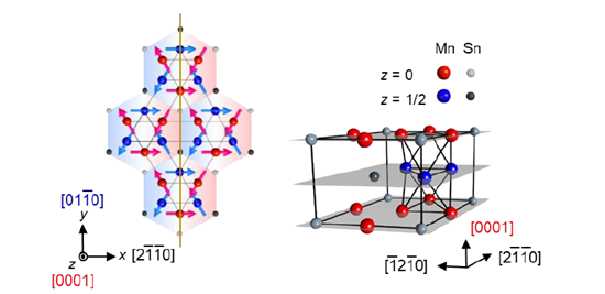
Fig. 1 Spin (left) and crystal structure (right) of the topological antiferromagnetic metal Mn3Sn
Further increasing the speed and density of magnetic memory
While pursuing the urge to miniaturize electronic devices while improving their functions, we have created communication and computational technology innovations that have changed our lives and the world. The milestones range from the smartphone that squeezed dozens of functions into one palm-sized device to the Internet of Things (IoT) that enables limitless connectivity around the globe. Yet as the digital transformation rapidly expands, it becomes clear that the ultimate constraint is power consumption, which ties in with environmental issues and severe costs. It is now time to rethink the best approach to developing future information processing and storage. Can we figure out a brand-new way to make it faster and more energy-efficient?
An emerging research field tackling this challenge is spintronics. Unlike conventional electronics that define binary logic using the electric charge of electrons, spintronic devices use electron spins to encode data. Since electron spins result in the magnetism of materials, a pure spin current (i.e., the flow of spin angular momentum without accompanying electric charge carriers) is a natural way to read and write information, rendering non-volatile magnetic memory that can store data for ages without requiring external power. However, one critical bottleneck for the widespread use of magnetic memory is a huge speed gap. The access time of magnetic memory is typically on a millisecond scale, over 10000 times slower than the main semiconductor-based memory used in today’s computers.
To resolve this issue, spintronic research is now evolving from its traditional realm based on ferromagnets toward antiferromagnets. The reading and writing speed of antiferromagnet-based devices can be two to three orders of magnitude faster (picosecond range) than that of ferromagnets (nanosecond range), which may dramatically reduce energy consumption, as energy is directly related to the operation speed. Moreover, antiferromagnets are nearly magnetization free, so they have no stray fields. This feature can effectively prevent cross-talks among neighboring components, which is particularly beneficial for realizing high-density integrations.
Meanwhile, the technology to detect and control electrical signals in all-antiferromagnetic MRAM is still in its early stages of development. One of the main challenges to address is the development of reading protocols. In particular, the transverse tunneling magnetoresistance (TMR), which is essential for the signal readout in conventional MRAM, has long been thought to require magnetization and therefore may be extremely difficult to achieve in antiferromagnetic devices.
Study of various properties of topological antiferromagnetic metals
(1) Demonstration of ultrafast spin dynamics in topological antiferromagnetic metals
Using Stroboscopic method*5, this study achieved time-resolved observation of spin dynamics in Mn3Sn using a very short laser pulse with about 0.1 picosecond pulse width (1 picosecond is a trillionth of a second). The measurement system is shown in Fig. 2. The results indicate that ultrafast spin switching is possible in the topological antiferromagnetic metal Mn3Sn.
*5 Stroboscopic method
A technique of detecting changes in fast-moving objects using short light pulses at regular intervals. The technique involves using a stroboscope that produces rapid flashes of light to light up the object in a way that makes it appear stationary or in slow motion.
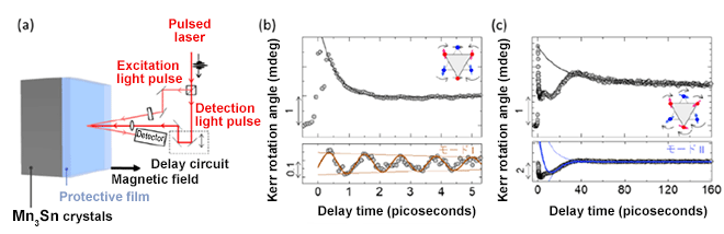
Fig. 2
(a) An illustration of the stroboscopic measurement system. A detection pulse is applied with a delay time to the excitation light pulse to detect spin dynamics in the topological antiferromagnetic metal Mn3Sn.
(b) Observations of oscillation mode I, in which neighboring spins are antiparallel. The oscillations occur with a rapid period of about 1 picosecond.
(c) Observations of oscillation mode II. This mode is similar to ferromagnets, where all spins move in the same direction.
The two modes shown in (b) and (c) arise from the dynamics of cluster magnetic octupoles in the topological antiferromagnet. Their ultrafast decay indicates that ultrafast spin switching is possible in the topological antiferromagnetic metal Mn3Sn.
(2) Piezomagnetic effect*2 allows information writing in antiferromagnet memory devices
Since its initial discovery by Edwin Hall more than a century ago, the anomalous Hall effect*3 is commonly believed to go hand in hand with magnetization while shying away from direct coupling with strain. Therefore, it seems unlikely to control the anomalous Hall effect with strain, but the topological antiferromagnet Mn3Sn provides a stage to make it happen. Using a piezoelectric strain apparatus with high tunability and accuracy (Fig. 3a), this study demonstrates that the sign and size of the nearly magnetization-free anomalous Hall effect in Mn3Sn can be changed by an applied strain as small as about 0.1% (Fig. 3b). This finding is a huge surprise because, for magnetic materials, a large strain on the order of 1% is typically necessary to induce any noticeable effect in electrical transport responses. This study further shows that Mn3Sn features a record-breaking room-temperature piezomagnetic effect*2 in a metallic state, which lies at the heart of the dramatic response of the anomalous Hall signal to applied strain.
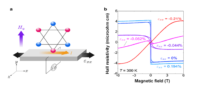
Fig. 3
(a) Schematic diagram illustrating the measurement configuration of the anomalous Hall effect under strain. Here, the Hall voltage VH generated along the z-axis direction of the sample is measured under tensile strain applied in the x direction. Hy denotes the external magnetic field, I represents the current, and εxx indicates the strain in the x direction.
(b) Magnetic field dependence of the Hall resistivity of Mn3Sn measured under various strains, εxx.
(3) World's first current control of the perpendicular binary states in antiferromagnets
In this study, experiments were conducted on multilayer thin films containing epitaxial thin films (crystalline thin films with neatly aligned atoms) of the topological antiferromagnet Mn3Sn and thin films of heavy metals.
Although the cluster magnetic octupole polarization*6 in the antiferromagnetic order of Mn3Sn can take six possible directions, the epitaxial strain in these thin films aligns the polarization perpendicular to the film surface, which provides the 1/0 binary states(Fig.4a and 4b).
By measuring the dependence of the Hall voltage signal on the write current at room temperature, this study shows that the Hall signal could be switched ~100 % with a write current of about 14 MA/cm2. This demonstrates the feasibility of perpendicular magnetic recording—a low-power and highly reliable recording technology employed in commercial magnetic memory devices — in an antiferromagnetic device.
*6 Magnetic octupole polarization
A cluster magnetic multipole is defined as a collective moment comprising a group of spins. In the case of Mn3Sn, to properly characterize the symmetry properties of its antiferromagnetic order, one needs to consider a basic unit that consists of six spins on adjacent kagome layers, namely, a cluster magnetic octupole. In other words, this antiferromagnetic order can be viewed as an order of the cluster octupoles, which is responsible for stabilizing the topological electronic band structure. Recent research has shown that, unlike ferromagnets, antiferromagnets' transverse transport properties, such as the anomalous Hall effect, are better characterized by the cluster magnetic multipole rather than the net magnetization. Similarly, in the MRAM device made of antiferromagnetic Mn3Sn, the device’s functionalities, such as the quantum tunneling magnetoresistance, are related directly to the magnetic octupole polarization.
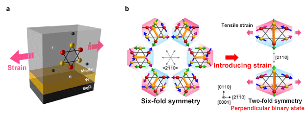
Fig. 4 Perpendicular binary state induced by tensile strain in the Kagome plane in the chiral antiferromagnet Mn3Sn.
(a) Schematic diagram of the multilayer film used in this study. Due to lattice mismatch between the Mn3Sn and the MgO substrate, tensile strain occurs in the Mn3Sn layer.
(b) The cluster magnetic octupole polarization of Mn3Sn has six-fold symmetry in the kagome plane.
However, by introducing the strain shown in Fig. 4a, the six-fold symmetry reduces to two-fold symmetry in the perpendicular direction to the film surface, resulting in perpendicular binary states.
(4) Discovery of a quantum tunneling magnetoresistance at room temperature
Currently, magnetic tunnel junctions (MTJs) with transverse tunneling magnetoresistance are used to read information in commercialized MRAM (Fig. 5). MTJs typically consist of a ferromagnetic layer, a tunnel barrier layer, and another ferromagnetic layer. The binary states "0" and "1" are generated by aligning the magnetization directions of the two ferromagnetic layers parallel or antiparallel to each other, respectively.
In this study, the ferromagnetic layer in MTJs was replaced with the antiferromagnet Mn3Sn, and for the first time, tunnel magnetoresistance was observed in MTJs composed entirely of antiferromagnets. The researchers also found that the change in magnetoresistance observed in these antiferromagnetic MTJs could be enhanced to the same extent (about 100%) as currently seen in ferromagnets, as predicted by theoretical calculations.
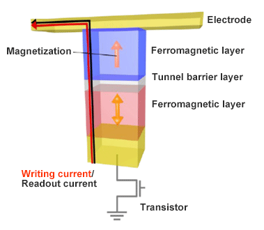
Fig. 5 Schematic diagram of MRAM and MTJ
A magnetic tunnel junction (MTJ) is typically composed of a ferromagnetic layer, a tunnel barrier layer, and another ferromagnetic layer. The orange arrows in the figure mark the direction of magnetization, and the yellow parts are the electrodes. By replacing the ferromagnetic layer with an antiferromagnet, the operating frequency of the MTJ can be improved, and miniaturization can be achieved.
Realization of next-generation electronic devices and their contribution to the post-semiconductor industry
The recent development of electronic devices based on topological antiferromagnetic metals has opened up new possibilities for ultrafast electronic devices with terahertz-scale operation speed. Such devices can be 10-100 times faster than current commercialized MRAMs. This breakthrough has the potential to revolutionize the field of information technology, by generating faster and more energy-efficient data storage. Moreover, advances in understanding and manipulation of antiferromagnetic ordered state may improve the performance of all-antiferromagnetic MRAM and thereby further accelerate the development of next-generation information technology.
The discovery of quantum tunneling magnetoresistance in antiferromagnetic MRAM devices brings them closer to practical applications. This breakthrough may strongly impact the future development of Japan's post-semiconductor industry.