Research Results
Contributing to energy saving of electric vehicles and industrial equipment
Significant performance improvement of SiC power semiconductorsFY2022
- Kimoto Tsunenobu (Professor, Graduate School of Engineering, Kyoto University)
- Program on Open Innovation Platform with Enterprises, Research Institute and Academia (OPERA)
- "Energy innovation based on innovative semiconductor technology that holds the key to the realization of an ultra-smart society" (2018-2022)
Significant performance improvement of SiC power semiconductors by developing interface defect reduction technology
Semiconductor devices based on Si (silicon) are not limited to data processing applications such as logic and memory devices for computers and communication equipment but are also widely used for "power control," such as motor control of electric vehicles and trains, transformers and DC-AC converters (power electronics). However, in the latter application, the power consumption (power loss) of the control circuit has become a major problem, and with the aim of reducing this loss, the development of transistors using SiC (silicon carbide), which has superior material properties compared with Si, has become more active in recent years. SiC power devices such as transistors and diodes have already started to come into practical use, such as the latest model N700S of the Shinkansen, which debuted in July 2020.
However, there are many defects in the oxide film-SiC boundary region (interface), which is the most important part of SiC transistors, and they have not been able to manifest their inherent high performance for 20 years or more. In August and September 2020, Professor Tsunenobu Kimoto's research group reported a unique method based on physical considerations, which significantly reduced interface defects and doubled the channel mobility of SiC transistors. In October 2021, this research was developed further, and the group succeeded in improving the characteristics by 6 to 80 times in practically important structures.
While aiming for a carbon-neutral world in the future, further performance improvement of SiC power devices is expected to meet increasing demands for advanced utilization of renewable energy, that is, highly efficient utilization of electric power energy.
Evolution of semiconductor power devices required by society
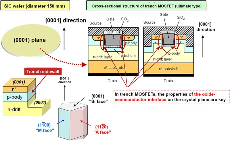
The most important transistor in semiconductors is a MOSFET (metal-oxide-semiconductor field effect transistor) that utilizes carrier transport at an oxide film - semiconductor junction (interface). The Si-MOSFET is a three-terminal device wherein the voltage applied to the gate electrode can change the electrical resistance between the two remaining electrodes (drain (D) and source (S)). In many applications, this transistor (MOSFET) is used as a switch between two states, an on-state and an off-state. In data processing, the on and off states are assigned to two values, 1 and 0, to perform calculations, and in power electronics, together with a diode and other parts, electric power is chopped and converted to a desired waveform to drive a motor or the like. Since it is necessary to control the energy (current) in power electronics, the electrical D-S resistance (on-resistance) becomes a loss when the transistor is turned on. The switch (current path [channel]) corresponds to the semiconductor interface adjacent to the oxide film, and to improve the efficiency of power electronics, "reducing the on-resistance," that is, reducing defects at the oxide-semiconductor interface, is key to improving performance.
Due to its basic material properties, SiC can handle higher voltage than Si and can open and close a switch at high speed, but the "on-resistance" that is directly related to the energy loss of the control circuit depends also on the crystal planes of the SiC semiconductor which form a channel. Practically, MOSFETs called "trench type" have been found to be the most promising, and in this device structure, it is necessary to form the core oxide film/SiC interface not on the SiC wafer surface ("Si face") but on a plane orthogonal to the wafer surface ("A face" or "M face"). Specifically, after engraving the wafer surface perpendicularly, an oxide film/SiC interface (channel) must be formed in the cross-section, and reduction of defects at this interface, with a more complicated device manufacturing process, is the second key to high functionality.
Invention of oxide film formation by non-oxidation (results of Professor Tsunenobu Kimoto's research group))
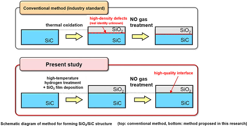
Si MOSFETs make use of a process where a high quality oxide film (SiO2) is formed on a Si surface by thermally oxidizing Si (heating to a high temperature in an oxygen atmosphere). This thermal oxide film is an insulating film with excellent electrical, mechanical, thermal, and chemical properties that is compatible with Si and is the basis of integrated circuit technology that is still making extraordinary progress today.
Like Si, SiC also has the property of forming a SiO2 film on the surface when it is thermally oxidized, which has been recognized as a major advantage of SiC, and SiC-MOSFETs have been manufactured by this method so far. However, an extremely large number of defects (more than 100 times that of Si) existed at the oxide film/SiC boundary (interface), and these interface defects greatly impaired the performance of SiC transistors. For many years, efforts have been made to reduce interface defects by adjusting the oxidation conditions of SiC and subsequent various heat treatment conditions, but no remarkable results had been obtained, and the origin of these interface defects had not been clarified.
Professor Kimoto's group has conducted experimental research with the seemingly contradictory goal of "forming a high-quality oxide film by a method that does not oxidize even one layer of SiC." As a result, they found that, for forming the oxide film on the SiC (0001) face ("Si face") , the following two points are effective in reducing defects, and actually reduced interface defects to about 1/5 compared to the conventional world standard (as of the time of the announcement in September 2020).
(1) In the process of oxidizing a SiC surface required to manufacture SiC transistors, the group noticed that high-density defects were introduced near the SiC surface, and found it was important to remove them by an appropriate method (hydrogen etching) before forming an oxide film.
(2) It was found that when high-quality SiC surface was formed by (1) and then an oxide film (SiO2 film) was formed by oxidation of SiC, high-density defects were newly generated. This problem was overcome by depositing an oxide film on the SiC surface, resulting in formation of a good quality oxide film.
Subsequently, Professor Kimoto's group developed this research and achieved epoch-making performance improvement in the transistor structure (crystal planes, impurity concentrations) which is important for practical use (announced in November 2021). The results are summarized by the following three points. The process used for oxide film/SiC interface formation is shown in the figure below.
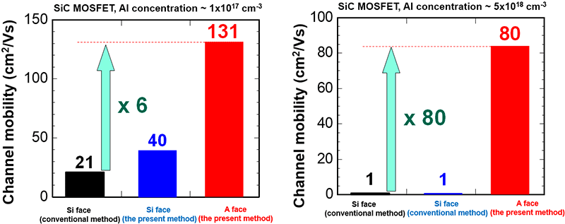
(1) An oxide film/SiC interface was formed on the crystal planes ("A face" and "M face") orthogonal to the wafer surface, which are required for high-performance SiC-MOSFETs (trench structure). In the experiments, A face and M face substrates were prepared, and SiC-MOSFETs were fabricated using the above original method. In this way, a six to seven times improvement in channel mobility was achieved compared to conventional MOSFETs with an oxide film on the Si face using the conventional oxide film formation method.
(2) In an actual SiC-MOSFET, it is necessary to form a MOS structure on the p-region to which a relatively high concentration of an acceptor impurity (aluminum) is doped in order to increase the blocking voltage and improve transistor reliability. As a result of fabricating MOSFETs on the A face and M face using heavily-doped p-type SiC used in production, channel mobility was improved by 6 to 80 times compared to conventional MOSFETs on the A face and M face.
(3) It is considered that in the case of the A face and M face, the performance improvement of (2) is due to superior flatness of the oxide film and the SiC interface, and the fact that electron scattering (interference with transport) is significantly reduced.
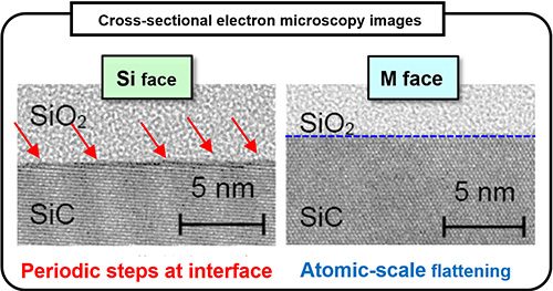
Cross-sectional electron micrograph of SiO2/SiC interface (with the M-plane, a flat interface is obtained at the atomic scale)
Promoting energy saving by putting SiC power semiconductors into practical use
In this research, through repeated ideas and experiments based on theory, oxide film/SiC interface defects, which had been regarded as the biggest obstacle in SiC power transistors, were significantly reduced.
The channel mobility of the SiC transistors was successfully increased by 6 to 80 times in practically important structures (crystal planes, impurity concentration). For manufacturers of SiC power semiconductors, this research method can be applied to the mass production of SiC-MOSFETs without the need for specialized new equipment or high-cost processes, and without additional capital investment. By applying these research results to trench-type SiC-MOSFET that significantly improves performance by miniaturization, it is possible to achieve (1) cost reduction by reducing the chip area and (2) improved reliability. In particular, the cost reduction (1) is expected to significantly accelerate the application of SiC-MOSFETs to power electronics, and at the same time, accelerate energy saving through wide adoption of SiC power semiconductors.
Currently, the global market for SiC power semiconductors is about 70 billion yen, but it is expected to exceed 200 billion yen in five years, and it is estimated that the increasingly widespread use of SiC power semiconductors will save energy equivalent to several nuclear power plants.
SiC-MOSFETs should be able to attain channel mobilities of 200 to 250 cm2/Vs, and it is hoped that basic university research, through the development of basic technologies like defect reduction, will further improve the performance of SiC power transistors.