- JST Home
- /
- Strategic Basic Research Programs
- /
 PRESTO
- /
- project/
- Nano Materials for New Principle Devices/
- [Nano materials devices] Year Started : 2023
[Nano materials devices] Year Started : 2023
Takamasa Kawanago
Ultra-low Voltage WSe2 CMOS Integrated Circuits
Researcher
Takamasa Kawanago

Senior Researcher
Semiconductor Frontier Research Center
National Institute of Advanced Industrial Science and Technology
Outline
This project will establish the fundamental technology for ultra-low voltage operating CMOS integrated circuits using tungsten diselenide (WSe2). For ultra-low voltage operation of WSe2 CMOS devices and circuits, this project will address the realization of double-gate operation in which the WSe2 channel is sandwiched between upper and lower gate stacks, construction of n/p FETs using non-doped WSe2 channels and development of a unique self-aligned process. Furthermore, this project also will apply the fabricated WSe2 CMOS devices for chip-level ultra-low voltage operating WSe2 CMOS integrated circuits.
Yui Sasaki
Development of nanodevices based on molecular self-assemblies
Researcher
Yui Sasaki

Lecturer
Research Center for Advanced Science and Technology
The University of Tokyo
Outline
Molecular self-assemblies can be driving forces to spontaneously fabricate functional nanostructures with high molecular orientation. This research aims to establish a methodology for the development of nanodevices based on molecular interactions.
Hirokazu Tahara
Development of efficient optoelectronic devices with quantum cooperativity in nanomaterial superstructures
Researcher
Hirokazu Tahara

Associate Professor
Faculty of Engineering
Yokohama National University
Outline
Collective nanomaterials can generate strong optical responses via their cooperative processes. In this research, I will develop optoelectronic devices with quantum cooperativity in collective nanomaterials to demonstrate efficient infrared-visible light-energy conversions. Nanomaterial superstructures are used to generate strong quantum cooperativity. I will clarify the mechanism of light-energy conversion in nanomaterial superstructures and establish methods for using quantum cooperativity in energy-conversion and information-conversion devices.
Takashi Tsuchiya
Creation of ultrafast iontronics
Researcher
Takashi Tsuchiya

Group Leader
Research Center for Materials Nanoarchitectonics
National Institute for Materials Science
Outline
While iontronics is a powerful method to explore untouched electronic functionalities of materials due to its capability of extremely high density electronic carrier accumulation by electric double layer effect, the slow operation speed has been limiting the range of application. In the present study, electric double layer response of iontronic devices is investigated in the view points of physical and chemical properties of components (electrolytes, channel semiconductors), interfaces, and device structures, in order to build a guiding principle for creation of ultrafast iontronic devices with various nanomaterials operating far faster than conventional ones.
Yusuke Nakanishi
Fabrication and characterization of one-dimensional heterojunctions inside nanospaces
Researcher
Yusuke Nakanishi

Assistant Professor
Graduate School of Science
Tokyo Metropolitan University
Outline
Atomically thin one-dimensional (1D) materials, known as ‘atomic wires’, which are typically fabricated inside nanospaces such as nanotubes, have emerged as promising components for nanoelectronic devices. However, their studies and applications have been severely hindered due to the difficulties in connecting electrodes. This study focuses on the fabrication and comprehension of the heterojunctions confined in 1D nanospaces to facilitate the integration of electrodes with atomic wires. Ultimately, the objective of this project is to pave the way for practical electronic applications of atomic wires.
Hiroyasu Nakayama
Highly reliable voltage-driven spintronic devices by interface engineering
Researcher
Hiroyasu Nakayama
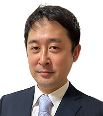
Senior Researcher
Research Center for Emerging Computing Technologies
National Institute of Advanced Industrial Science and Technology
Outline
In the super smart society of the future, there are concerns about a huge increase in power consumption as the number of IoT devices increases rapidly. Therefore, a computer system that operates with lower power consumption is desired to be achieved. From the viewpoints of high-speed operation, non-volatility, and low write power consumption, voltage control of spins is a promising technology for next-generation memory devices. However, there is a fatal problem with the high write error rate in conventional dynamic method. This project aims to create a novel method for voltage control of spins with much higher reliability by exploiting long-range interactions those act on the ultrathin magnetic films and their interfaces.
Naoki Higashitarumizu
Large-scale mid-infrared optoelectronics based on narrow-gap 2D materials
Researcher
Naoki Higashitarumizu
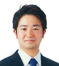
Exceptional Principal Investigator
Electrical Engineering and Computer Sciences
University of California at Berkeley
Outline
The growing demand for mid-infrared light has gained prominence across various applications, including gas sensing, night vision, disaster prevention and security, building maintenance, and automotive technologies. In this project, my focus lies in harnessing the exceptional optical characteristics exhibited by narrow-gap 2D semiconductors. The overarching goal is to pioneer the development of novel materials and innovative processes that will yield superior performance in mid-infrared optoelectronic devices. This research endeavors span not only the single device on a microscale but also encompass the large area integrations on a chip to wafer scale.
Toshinori Matsushima
Enhanced carrier transport in two-dimensional perovskites
Researcher
Toshinori Matsushima
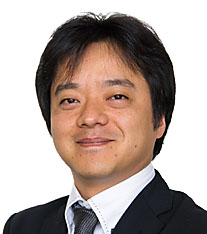
Associate Professor
International Institute for Carbon-Neutral Energy Research
Kyushu University
Outline
Field-effect transistors with a two-dimensional perovskite semiconductor layer containing carrier-transporting organic amines are fabricated. This innovative approach enables ambipolar operation by dividing carrier transport between the organic amine layer and the metal halide layer. Through the optimization of the perovskite film fabrication processes, grain boundary density and defect density are reduced, thus accelerating carrier transport.
Masakazu Matsubara
Creation of opto-spintronic functionalities by controlling the symmetry of nanospace
Researcher
Masakazu Matsubara
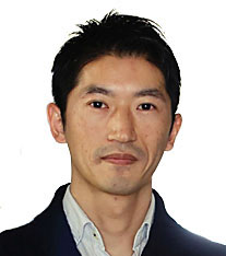
Associate Professor
Graduate School of Science
Tohoku University
Outline
The various functionalities exhibited by materials are closely linked to the symmetry of their inherent electronic degrees of freedom. In this research, I will develop various thin-film artificial materials with manipulated nanospace symmetry ―two-dimensional metamaterials- and establish fundamental technologies for creating novel opto-spintronic functionalities that are not bound by the intrinsic properties of materials, such as optical spin current generation/control and spin photoelectric conversion based on new principles.
Masataka Mogi
Emergent topological properties from thin film interface and structural heterogeneity
Researcher
Masataka Mogi

Assistant Professor
Faculty of Engineering
University of Tokyo
Outline
Spatially inhomogeneous structures, known as moiré superlattices, emerge from twisted two-dimensional materials, leading to unconventional electronic and optical responses. In this research program, I extend the concept of spatial inhomogeneity in quantum matter using advanced molecular beam epitaxy techniques, aiming to explore new electronic functionalities that utilize topological states of matter. Specifically, I develop novel methods to create superstructures that are distinct from moiré superlattices, achieved through the design of interfacial strain or compositional control. Furthermore, I aim to realize a novel light-induced topological phase switch via highly nonequilibrium states using advanced ultrafast laser techniques.


