News & Topics
Novel fabrication method for microfluidic devices
START Project Promotion Type (Commercialization Support)
Department of Industry-Academia Collaboration
https://www.jst.go.jp/start/en/jigyo/index.html
A research team at Kyoto University’s Institute for Integrated Cell-Material Sciences (iCeMS) led by Professor Easan Sivaniah, has advanced the miniaturization of the Organized Microfibrillation (OM) technology under the framework of START Project Promotion Type (Commercialization Support). Based on this technology, they have developed an innovative process for fabricating microfluidic devices. The achievement was published in Nature Communications on May 19, 2022.
(DOI: 10.1038/s41467-022-29956-4)
Microfluidic devices are chip-type platforms with functionality provided by microfluidic channels. Such devices are typically made from resin and glass and can freely mix or divide liquids and particle mixtures flowing at the microscale. This technology is expected to have a wide range of applications in drug discovery, healthcare, chemical synthesis of minute quantities, genetic analysis, etc.
In the conventional method, the substrate is etched and then sealed against another plastic or glass cover to create an enclosed channel. However, defects such as wrinkles and blockages are likely to occur during the sealing process when thin film resins are used. It has been an obstacle to create fine and thinner microfluidic devices.
Features of the new method are as follows:
・Channels printed with the OM technique create a structural color effect.
The OM technology is able to generate pores in polymer films. The position of these pores causes a special reflection of light, giving it a structural color. The pores are also connected over long distances and can be printed to make porous channels.
・Simplified the production process from two steps to one step.
With the OM technology, pores can be directly printed or formed inside the resin, so the sealing step can be omitted.
・Achieved the finest and thinnest printing method in the world.
Harnessing the OM technology, an ultra-high quality printing technology with a resolution of up to 14,000 dpi, the team realized the microchannel printing with a minimum width of 5μm and device thickness down to 1μm. (1μm=0.001mm) Furthermore, this one step method with no sealing process avoids the problem of wrinkles and cracks forming during the sealing of thin films.
Film-type microfluidic devices are made significantly thinner and miniaturized by the new method, and it is expected to be applied to flexible and wearable devices, such as a health monitoring system attaching tiny patches. The research team has engaged in research and development aimed at the promotion of inkless printing. These days, printing methods are not limited to just making color. This research demonstrated the great potential of applying the OM printing technology to other fields. The team aims to explore new markets through the application of the microfluidic devices as well as promoting the inkless printing development.
Kyoto University Press Release:https://www.icems.kyoto-u.ac.jp/en/news/7375/
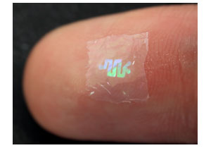
The microfluidic device printed on a polystyrene film with 1μm thickness. It is transparent but colored due to structural color properties.
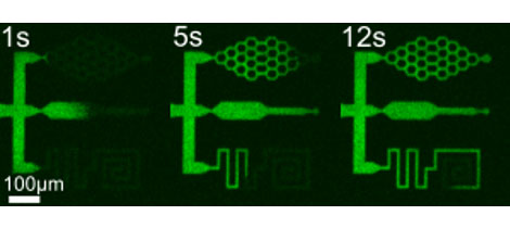
Solvent flow in the microchannel fabricated in this study. It is colored with a green fluorescent marker for clarity. The minimum channel width is 5 μm.