Optical anomaly induced by surface plasmon polariton (SPP) is one of the “classical” research subjects. However, it has been a rich research field giving many interesting phenomena in photonics, physics, and chemistry. A classical example is a spectral dip in diffracted light from a grating, known as ‘Wood’s anomaly’, which was discovered more than 100 years ago. The latest example is an extraordinary optical transmission through sub-wavelength hole arrays, reported by Ebbesen et al in 1998. This discovery sparked intensive studies on SPP-based nano-structured optics. ‘Plasmonics’ is the name of the new field of applications utilizing SPP, which can break through the limits in speed and downsizing of today’s conventional electronics and photonics. Optical digital signals are converted to SPPs at the entrance of an integrated SPP circuit, then processed, and re-converted to optical signal to extract the result. To date, a variety of SPP optical elements such as lenses, mirrors, beam splitters, interferometers, and resonators have been reported.
We explore SPP dynamics in nano metal structures using interferometric time-resolved photoemission electron microscopy (ITR-PEEM). ITR-PEEM movies reveal the spatio-temporal evolution of SPP with 0.33 fs frame separation and 50 nm spatial resolution. Excitation light is the second harmonic of Ti: sapphire laser oscillator with 10 fs pulse width and 400 nm center wavelength. Phase correlated pump-probe pulse pairs are generated by splitting fs-pulses through a Mach-Zehnder interferometer (MZI). The delay time between pump and probe ( ) is controlled at an accuracy of <50 as (<1/25 ) is controlled at an accuracy of <50 as (<1/25  ). The laser pulses are focused on a sample placed at a focal plane of PEEM. Two-photons give electrons energy to overcome the work function of sample and induce photoemission, whose spatial distribution reveals the nonlinear map of the surface plasmon field. We track the time evolution of SPP fields using a pump-probe method.
We have taken movies of localized [1] and propagating SP modes [3] on silver gratings, and propagating SPP on deposited silver films [2]. Figure 1 shows selected frames of an ITR-PEEM movie of a propagating SPP from a one-dimensional defect (groove) in a silver film ( : 0 ? 46.7 fs). Laser lights coming from the left side of each frame couple to the SPP mode at the right edge of the groove. The propagation of SPP is pictured as an advancement of the wave front of an oscillatory pattern as increases. By comparing with a simulation, the propagation length, lifetime, and group velocity of SPP are determined to be 3 ). The laser pulses are focused on a sample placed at a focal plane of PEEM. Two-photons give electrons energy to overcome the work function of sample and induce photoemission, whose spatial distribution reveals the nonlinear map of the surface plasmon field. We track the time evolution of SPP fields using a pump-probe method.
We have taken movies of localized [1] and propagating SP modes [3] on silver gratings, and propagating SPP on deposited silver films [2]. Figure 1 shows selected frames of an ITR-PEEM movie of a propagating SPP from a one-dimensional defect (groove) in a silver film ( : 0 ? 46.7 fs). Laser lights coming from the left side of each frame couple to the SPP mode at the right edge of the groove. The propagation of SPP is pictured as an advancement of the wave front of an oscillatory pattern as increases. By comparing with a simulation, the propagation length, lifetime, and group velocity of SPP are determined to be 3  , 12 fs, and 0.61 c (c: speed of light), respectively.
Our method can be applied for observations of wave packet dynamics in more complicated SPP circuits. Now the research is directed to the SPP dynamics in nano-scale circuits fabricated by using focused ion beam and electron beam lithography techniques. , 12 fs, and 0.61 c (c: speed of light), respectively.
Our method can be applied for observations of wave packet dynamics in more complicated SPP circuits. Now the research is directed to the SPP dynamics in nano-scale circuits fabricated by using focused ion beam and electron beam lithography techniques.
Reference:
• “Femtosecond Imaging of Surface Plasmon Dynamics in a Nanostructured Silver Film” A. Kubo, K. Onda, H. Petek, Z. Sun, Y. S. Jung, H. K. Kim, Nano Lett. 5, 1123 (2005)
• “Femtosecond microscopy of surface plasmon polariton wave packet evolution at the silver/vacuum interface” A. Kubo, N. Pontius, and H. Petek, Nano Lett. 7, 470 (2007)
• “Femtosecond microscopy of localized and propagating surface plasmons in silver gratings” A. Kubo, Y. S. Jung, H. K. Kim and H. Petek, J. Phys. B 40, S259 (2007)
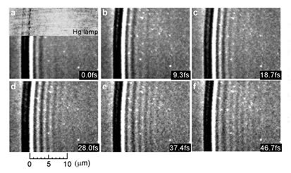
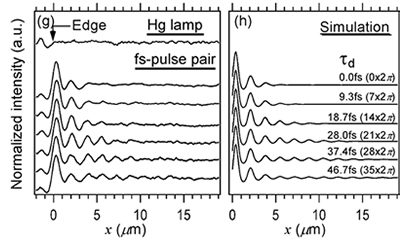
Fig.1 : ITR-PEEM movie of a propagating surface plasmon in a deposited silver film. (a-f): selected frames of the movie from the range of at 0 ? 46.7 fs. The interval of each frame is 9.3 fs. Inset of (a) shows the surface topography obtained by using a conventional Hg-lamp excitation. (g): Cross sections of (a-f). (h): Corresponding simulations of (g). As a consequence of SPP propagation from the edge, the position of the wave front of oscillatory pattern advances as increases ( : 0-37.4 fs). The amplitude of the pattern attenuates at =46.7 fs due to a decay of SPP.
|