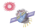
新規酸窒化物を用いたピエゾ電界誘起量子井戸型太陽電池の創製
板垣 奈穂
論文
- S. Bornholdt, N. Itagaki, K. Kuwahara, H. Wulff,M. Shiratani and H. Kersten,
"Characterization of the energy flux toward the substrate during magnetron sputter deposition of ZnO thin films",
Plasma Sources Sci. Technol., Vol. 22, Issue 2, p. 025019 (2013). - David C. Look,
"Model for thickness dependence of mobility and concentration in highly conductive zinc oxide",
Optical Engineering Vol. 52 Issue 3, p. 033801 (2013). - I. Suhariadi, K. Matsushima, K. Kuwahara, K,
"Effects of Hydrogen Dilution on ZnO Thin Films Fabricated via Nitrogen Mediated Crystallization",
Japanese Journal of Applied Physics., Vol. 52, p. 01AC08 (2013). - I. Suhariadi, N. Itagaki, K. Kuwahara, K,
"ZnO:Al Thin Films with Buffer Layers Fabricated via Nitrogen Mediated Crystallization: Effects of N2/Ar Gas Flow Rate Ratio",
Transactions of the Materials Research Society of Japan, Vol. 37, p. 165 (2012). - Kazunari Kuwahara, Naho Itagaki, Kenta Nakahara, Daisuke Yamashita, Giichiro Uchida, Kunihiro Kamataki, Kazunori Koga, and Masaharu Shiratani,
"High quality epitaxial ZnO films grown on solid-phase crystallized buffer layers",
Thin Solid Films, Vol. 520, Issue 14, p. 4674 (2012).
口頭発表・ポスター発表
- Naho Itagaki,
"Sputtering growth of ZnO-based semiconductors using ZnON buffer layers for optoelectronic applications",
International Symposium on Plasma-Nano Materials and Processes, Seoul, Korea, 2014/4/3. - N. Itagaki,
"Sputtering growth of single-crystalline ZnO-based semiconductors on lattice mismatched substrates",
SPIE(international society for optics and photonics) photonics west 2013, San Francisco, USA, 2014/2/3. - 板垣奈穂、
「ZnInON系太陽電池材料の探索」、
第5回薄膜太陽電池セミナー2013,名古屋、2013/11/15. - N. Itagaki,
"Sputter deposition of high quality ZnO based semiconductors in Ar/N2 atmosphere (tentative)",
The 9th Asian-European International Conference on Plasma Surface Engineering, Jeju, korea, 2013/8/25. - N. Itagaki,
"Novel Application of Ar/N2 Discharges to Sputtering Growth of High Quality Oxide Semiconductors",
The XXXI edition of the International Conference on Phenomena in Ionized Gases, Granada, Spain, 2013/7/14. - Naho Itagaki, Kazunari Kuwahara, Kouichi,
"Sputter Deposition of Semiconductor-Grade ZnO Based Materials on Lattice Mismatched Substrates for Optoelectronic Applications",
The Collaborative Conference on Materials Research 2013, Jeju, Korea, 2013/6/24. - N. Itagaki, K. Kuwahara, K. Matsushima, K. Oshikawa
"Novel fabrication method for ZnO films via nitrogen-mediated crystallization ",
International society for optics and photonics(SPIE) photonics west 2012(San Francisco, USA), 2012/1/22
出版物
その他
プレス発表
受賞
- 板垣奈穂、
4th International Symposium on Advanced Plasma Science, Best Presentation Award
“Ineteraction between amplitude modulated reactive plasmas and nanoparitcles grown in the plasmas”
(2012年度) - 板垣奈穂、
11th Asia Pacific Conference on Plasma Science and Technology & 25th Symposium on Plasma Science for Materials, ”Advanced Plasma Application
“Zinc-Indium Oxynitride Thin Films for Multiple-Quantum-Well Solar Cells”
(2012年度)


