![]()
![]()

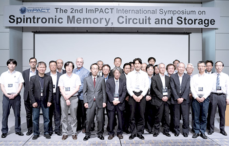
| 会議名称 | ImPACT佐橋プログラム 第2回 国際シンポジウム (The 2nd 【ImPACT】 International Symposium on Spintronic Memory, Circuit and Storage) |
|---|---|
| 開催日時 | 2016年9月30日(金曜) |
| 会場 | つくば国際会議場 / 〒305-0032 茨城県つくば市竹園2丁目20-3 |
| シンポジウム会場 | 中ホール300 |
| Discussion and Poster Session with Welcome Reception会場 |
多目的ホール |

| 9:00-9:10 | Opening Remarks | |
|---|---|---|
| Prof. Masashi SAHASHI | ImPACT Program Manager (Tohoku University) | |
| 9:10-9:40 | Greeting | |
| Dr. Kazuo KYUMA | Council Member for Science, Technology and Innovation, Cabinet Office, Government of Japan | |
| Dr. Michiharu NAKAMURA | Counselor to President of JST (Former President) | |
| Dr. Ryoji CHUBACH | President of AIST | |
| 9:40-10:10 | Embedded MRAM for Now and the Future: Innovating Ultra Low Energy Systems |
|
|---|---|---|
| Dr. Seung H. Kang | Qualcomm Technologies, Inc., USA | |
| 10:10-10:40 | Perpendicular STT-MRAM for Embedded Applications | |
| Dr. Po-Kang Wang | TDK-Headway Technologies, Inc., USA | |
| 10:40-11:10 | MRAM-Bringing Benefits to Applications Today | |
| Mr. Joe. O’Hare | Everspin Technologies, Inc., USA | |
| 11:10-11:40 | pMTJ STT-MRAM Technology and Manufacturing | |
| Dr. Yiming Huai | Avalanche Technology, USA | |
| 11:40-12:10 | Near-future STT-MRAM Applications from IoT to Cloud and Their Respective Memory Hierarchies |
|
| Dr. Shinobu FUJITA | Toshiba Corporation, Japan | |
| 12:10-12:30 | Short Summary | |
| 12:30-14:00 | Lunch | |
| 14:00-14:30 | The Integration of IoT and Machine Learning will Bring out the Autonomous Driving and Trigger the Restructuring of Many Industries. |
|
|---|---|---|
| Dr. Tsuguo NOBE | Intel Corporation, Japan | |
| 14:30-15:00 | NanoBridge-FPGA for IoT Era | |
| Dr.Toshitsugu SAKAMOTO | NEC Corporation, Japan | |
| 15:00-15:30 | Storage Class Memory/NAND Flash Hybrid Storage System | |
| Prof. Ken TAKEUCHI | Chuo University, Japan | |
| 15:30-16:00 | Coffee Break | |
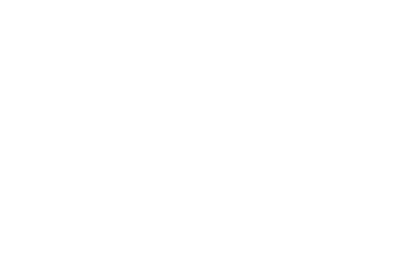
▲ Greeting 久間議員(CSTI)
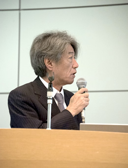
▲ Greeting 中村顧問(JST)

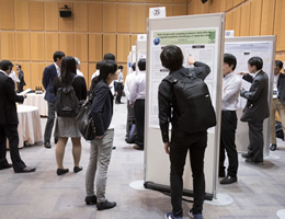
▲ 会場風景
| 16:00-16:30 | Electric-field-controlled MRAM: Device and Circuit Development | |
|---|---|---|
| Prof. Pedram Khalili-Amiri | UCLA , Inston Inc., USA | |
| 16:30-17:00 | Nanoscale Two- and Three Terminal Spintronics Devices for VLSI | |
| Prof. Hideo OHNO | Tohoku University, Japan | |
| 17:00-17:30 | Emerging Three-Terminal Magnetic Memory Devices | |
| Prof. Kyung-Jin Lee | Korea University, Korea | |
| 17:30-18:00 | Voltage-induced Anisotropy Change for Voltage-driven MRAM | |
| Dr. Shinji YUASA | AIST, Japan | |
| 18:00-18:30 | Short Summary | |
| 18:30-21:00 | Discussion and Poster Session with Welcome Reception | |
| 21:00 | Closing Remarks | |

| 01 | Outline of ImPACT Sahashi Program Masashi Sahashi (Program Manager, Tohoku Univ.) |
|---|---|
| 02 | Overview of spintronic integrated circuit project Hideo Ohno, Tetsuo Endoh, Takahiro Hanyu, Shoji Ikeda (Tohoku Univ.) |
| 03 | Scheme of ImPACT Voltage-Torque MRAM Project Shinji Yuasa (AIST) |
| 04 | Simulation Support Team Hiroshi Imamura1, Masafumi Shirai2, Tatsuki Oda3, Kohji Nakamura4, Yoshio Miura5 (1AIST, 2Tohoku Univ., 3Kanazawa Univ., 4Mie Univ., 5KIT) |
| 05 | Two- and three-terminal devices for spintronics based integrated circuits H. Sato, S. Fukami, S. Ikeda, and H. Ohno (Tohoku Univ.) |
| 06 | Magnetic properties of MgO/FeV/MgO and MgO/Fe/FeV/Fe/MgO structures for spintronics integrated circuits M. Bersweiler, K. Watanabe, E. C. I. Enobio, H. Sato, S. Fukami, F. Matsukura, and H. Ohno (Tohoku Univ.) |

▲ 会場風景
| 07 | Spin-orbit torque induced magnetization switching in nano-scale Ta/CoFeB/MgO dots C. Zhang, S. Fukami, H. Sato, F. Matsukura, and H. Ohno (Tohoku Univ.) |
|---|---|
| 08 | A 600-μW ultra-low-power associative processor based on MTJ nonvolatile memories with autonomic intelligent power-gating scheme Y. Ma, S. Miura, H. Honjo, S. Ikeda, T. Hanyu, H. Ohno, and T. Endoh (Tohoku Univ.) |
| 09 | Design of an MTJ-Based Nonvolatile LSI for Energy-Efficient Microcontroller Unit M. Natsui, A. Tamakoshi, T. Endoh, H. Ohno, and T. Hanyu (Tohoku Univ.) |
| 10 | Design of an MTJ-Based Nonvolatile Flip-Flop with High-Sensitive Self-Terminated Writing for a Nonvolatile Microcontroller Unit Daisuke Suzuki and Takahiro Hanyu (Tohoku Univ.) |
| 11 | Voltage-controlled magnetic anisotropy in epitaxial Cr/ultrathin Fe/MgO/Fe magnetic tunnel junctions Takayuki Nozaki1, Anna Kozioł-Rachwał1,2, Witold Skowroński1,2, Vadym Zayets1,Yoichi Shiota1, Shingo Tamaru1, Hitoshi Kubota1, Akio Fukushima1, Shinji Yuasa1, and Yoshishige Suzuki1,3 (1AIST, 2AGH Univ., 3Osaka Univ.) |
| 12 | Evaluation of write error rate of voltage-driven dynamic magnetization switching Yoichi Shiota1, Takayuki Nozaki1, Shingo Tamaru1, Tomohiro Taniguchi1, Kay Yakushiji1, Hitoshi Kubota1, Akio Fukushima1, Shinji Yuasa1, and Yoshishige Suzuki1,2 (1AIST, 2Osaka Univ.) |
| 13 | High Magnetoresistance in Fully Epitaxial Magnetic Tunnel Junctions with a Semiconductor GaOx Barrier Narayananellore Sai Krishna1, Norihiro Matsuo1,2, Naoki Doko1,2, Hidekazu Saito1, and Shinji Yuasa1 (1AIST, 2CIT) |
| 14 | Wafer Direct Bonding for Layer Transfer of Magnetic Tunnel Junctions H. Takagi, Y. Kurashima, A. Maeda, K. Yakushiji, and S. Yuasa (AIST) |
| 15 | Development of Three-Dimensional Integration Technology for perpendicular-type STT-MRAMs K. Yakushiji, H. Takagi, N. Watanabe, A. Sugihara, Y. Kurashima, K. Kikuchi and S. Yuasa (AIST) |
| 16 | Circuit design policy of Voltage Controlled MRAM (VCM) for Ultra Large Last Level Cache Keiko Abe1, Hiroki Noguchi1, Kazutaka Ikegami1, Shinobu Fujita1, Yoichi Shiota2, Takayuki Nozaki2, Shinji Yuasa2 and Yoshishige Suzuki2 (1Toshiba, 2AIST) |
| 17 | Study of CoFeB/Mg1-xTixO magnetic tunnel junctions: tunneling magnetoresistance and voltage effect on perpendicular magnetic anisotropy Yoichi Shiota1, Takayuki Nozaki1, Shingo Tamaru1, Tomohiro Taniguchi1, Kay Yakushiji1, Hitoshi Kubota1, Akio Ikhtiar1,2, K. Mukaiyama1, S. Kasai1, P.-H. Cheng1,2, T. Ohkubo1, Y. K. Takahashi1, T. Furubayashi1, and K. Hono1,2 (1NIMS, 2Univ. of Tsukuba) |
| 18 | Lattice-matched Co2FeAl/cation-ordered MgAl2O4/Co2FeAl Magnetic Tunnel Junctions with Large Tunnel Magnetoresistance exceeding 300% Thomas Scheike, H. Sukegawa, K. Inomata, T Ohkubo, K. Hono and S. Mitani (NIMS) |
| 19 | Spin dependent transport in Heusler-alloy-based magnetic junctions with semiconducting Cu(In0.8Ga0.2)Se2 spacer Koki Mukaiyama1, K. Masuda1, S. Kasai1,2, Y. K. Takahashi1, P-H.Cheng1,3, Ikhtiar1,3, Y. Miura1,4, T. Ohkubo1, S. Mitani1,3, and K. Hono1,3 (1NIMS, 2RIKEN, 3Univ. of Tsukuba, 4KIT) |
| 20 | Giant tunnel magnetoresistance in epitaxial Fe/MgAl2O4/Fe(001) magnetic tunnel junctions prepared by a direct sputtering technique Mohamed Belmoubarik, Hiroaki Sukegawa, Tadakatsu Ohkubo, Seiji Mitani, Tadakatsu Okubo and Kazuhiro Hono (NIMS) |
| 21 | Realization of high quality epitaxial current-perpendicular-to-plane giant magnetoresistive pseudo spin-valves on Si(001) wafer using NiAl buffer layer iamin Chen1,2, J. Liu2, Y. Sakuraba2, H. Sukegawa2, S. Li2 and K. Hono2,1 (1Univ. of Tsukuba, 2NIMS) |
| 22 | Electric-field effect on FePt|MgO junction studied by x-ray spectroscopy S. Miwa1, M. Suzuki2, K. Matsuda1, T. Nozaki3, K. Tanaka1, E. Tamura1, S. Yuasa3, Y. Suzuki1 (1Osaka Univ., 2JASRI, 3AIST) |
| 23 | Enhancement of voltage induced interfacial Dzyaloshinskii-Moriya interaction at Fe|MgO by one monolayer insertion of Pt Kohei Nawaoka1, Shinji Miwa1, Takayuki Nozaki2, Minori Goto1, Eiichi Tamura1, Shinji Yuasa2, Yoshishige Suzuki1 (1Osaka Univ., 2AIST) |
| 24 | Voltage induced changes of spin wave modes in disk-shaped CoB/FeB nanomagnet Jaehun Cho1, Shinji Miwa1, Kay Yakushiji2, Shingo Tamaru2, Hitoshi Kubota2, Akio Fukushima2, Shinji Yuasa2, and Yoshishige Suzuki1,2 (1Osaka Univ., 2AIST) |
| 25 | Magnetic tunnel junctions using ultrathin L10-ordered MnGa electrodes K. Z. Suzuki1, R. Ranjbar1, J. Okabayashi2, Y. Miura3, A. Sugihara1, H. Tsuchiura4, and S. Mizukami1 (1Tohoku Univ. WPI-AIMR, 2Univ. of Tokyo, 3KIT, 4Tohoku Univ.) |
| 26 | Current-induced magnetization switching in MnGa/Pt film with perpendicular magnetization R. Ranjbar, K. Z. Suzuki, Y. Sasaki, L. Bainsla, and S. Mizukami (Tohoku Univ.) |
| 27 | Material and process for 10 nm order MRAM with voltage-controlled magnetic anisotropy Naoharu Shimomura1, Yuichi Ohsawa1, Yushi Kato1, Chikayoshi Kamata1, Yuuzo Kamiguchi1, Satoshi Shirotori1, Tomoaki Inokuchi1, Tadaomi Daibo1, Altansargai Buyandalai1, Junichi Ito1, Hiroaki Sukegawa2, Seiji Mitani2, Kazuhiro Hono2 and Hiroaki Yoda1 (1Toshiba, 2NIMS) |
| 28 | Material and process for 10 nm order MRAM with voltage-controlled magnetic anisotropy Naoharu Shimomura1, Yuichi Ohsawa1, Yushi Kato1, Chikayoshi Kamata1, Yuuzo Kamiguchi1, Satoshi Shirotori1, Tomoaki Inokuchi1, Tadaomi Daibo1, Altansargai Buyandalai1, Junichi Ito1, Hiroaki Sukegawa2, Seiji Mitani2, Kazuhiro Hono2 and Hiroaki Yoda1 (1Toshiba, 2NIMS) |
| 29 | An efficient X-ray fluorescence detection system for high-precision X-ray absorption and magnetic circular dichroism spectroscopy in ultrathin films Motohiro Suzuki, Yoshinori Kotani, Naruki Tsuji, and Tetsuya Nakamura (JASRI) |
| 30 | Simulation of magnetization switching utilizing voltage-induced changes of magnetic anisotropy and Dzyaloshinskii-Moriya interaction Hiroshi Imamura, T. Nozaki, S. Yuasa, Y. Suzuki (AIST) |
| 31 | Huge electric-field modulation of the magnetic anisotropy energy of the 5d transition-metal monolayer on the Fe(001) and Co(111) surfacey Masahito Tsujikawa and Masafumi Shirai (Tohoku Univ.) |
| 32 | Fe thickness dependence of magnetic anisotropy energy and electric field variation in Cr/Fe/MgO Tatsuki Oda, Tomosato Kanagawa, Nurul Ikhsan, Masao Obata (Kanazawa Univ.) |
| 33 | A first-principles study on the voltage control of magnetic damping constant in Fe(001) surface and Fe/MgO(001) interface Yoshio Miura (KIT) |
| 34 | Theoretical study on tunneling magnetoresistance of L10-MnGa based magnetic tunnel junctions Yoshio Miura (KIT) |
| 35 | Role of spin-orbit coupling in electric field effect on magnetocrystalline anisotropy of metal thin films Kohji Nakamura (Mie Univ.) |
| 36 | Research scope of the Center for Spin-Orbitronic Materials in Korea for nonvolatile memory applications Young Keun KIM (Korea Univ.) |

総数207名
(日本国内 190名、プレス関連(2社 2名)、国外(6カ国) 17名(アメリカ5名、韓国4名、台湾4名、中国2名、シンガポール1名、ベルギー1名)
●主な一般参加者ご所属一覧 約40機関が参加:
アドバンテスト、キヤノンアネルバ、EIDEC、エイコー、富士通、北海道大学、インテル、KEYSIGHT TECHNOLOGIES、Lapisセミコンダクタ、LG、Micron Memory、日本タングステン、日新イオン機器、Samsung、昭和電工、ソシオネクスト、ソニー、田中貴金属、TDK、TEL、日本磁気学会、東陽テクニカ、豊田工業大学、UBE、東京大学、筑波大学、ウィンボンド・エレクトロニクス、Chinese academy of science、Hanyang Univ.、Etron Technology、Feng Chia Univ.、National Taiwan Univ.、Industrial Technology Research Institute、National University of Singapore、IMEC 他
Organized by [ImPACT] SAHASHI program, Japan Science and Technology Agency
Copyright © 2016 Japan Science and Technology Agency. All Rights Reserved.
