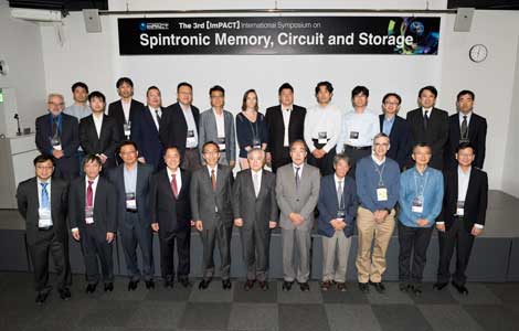
| 会議名称 | ImPACT佐橋プログラム 第3回 国際シンポジウム (The 3rd 【ImPACT】 International Symposium on Spintronic Memory, Circuit and Storage) |
|---|---|
| 開催日時 | 2017年9月23日(土)~25日(月) |
| 会場 | 東北大学 青葉山キャンパス / 〒980-8579 宮城県仙台市青葉区荒巻字青葉6-6 |
| シンポジウム会場 | カタールホール |
| Discussion and Poster Session with Welcome Reception会場 |
工学部 中央棟 1F DOCK |
|
|

| 9:30-9:40 | Opening Remarks | |
|---|---|---|
| Prof. Masashi SAHASHI | ImPACT Program Manager (Tohoku University) | |
| 9:40-10:10 | Welcome Notes | |
| Dr. Yuko Harayama | CSTI, Cabinet Office, Government of Japan | |
| Dr. Michiharu Nakamura | Counselor to President of JST (Former President) | |
| Prof. Susumu Satomi | President, Tohoku University | |
| 10:10-10:50 | Future Mobility Innovation by Vehicle Electrification and Intelligence | |
|---|---|---|
| Dr. Kazuhiro Doi | NISSAN MOTOR, Japan | |
| 10:50-11:30 | Spintronics Nanodevices for Low-power Integrated Circuits | |
|---|---|---|
| Prof. Hideo Ohno | Tohoku University, Japan | |
| 11:30-12:10 | Materials and Processes for Voltage-Torque MRAM | |
| Dr. Shinji Yuasa | AIST, Japan | |
| 12:10-12:50 | Electric-field controlled nucleation of magnetic skyrmions at room temperature | |
| Dr. Hélène Béa | SPINTEC, France | |
| 13:00-13:40 | Near-future MRAM applications: Emerging big market can be created? | |
|---|---|---|
| Dr. Shinobu Fujita | Toshiba, Japan | |
| 14:45-15:25 | An Implementation of Ultra-Low-Standby Power SRAMs using 65 nm Silicon-on-Thin-Box (SOTB) for Smart IoT | |
|---|---|---|
| Dr. Koji Nii | Renesas Electronics, Japan | |
| 15:25-16:05 | Non-Volatile Memory Technologies for Present and Future Applications | |
| Dr. Kazunari Ishimaru | Toshiba Memory, Japan | |
| 16:05-16:25 | Coffee Break | |
| 16:25-17:05 | CMOS-embedded STT-MRAM Technology in 2x nm Nodes for GP-MCU | |
|---|---|---|
| Dr. Danny P. Shum | Globalfoundries, Singapore | |
| 17:05-17:45 | Challenges in Resistive Memory Enabled Circuits and Systems: Memory, Nonvolatile Logics and AI Chips | |
| Prof. Meng-Fan Chang | National Tsing Hua University, Taiwan | |
| 17:45-20:00 | Discussion and Poster Session with Welcome Reception | |
| 20:00 | Closing (Day1) | |
▲ Welcome Notes 原山議員(CSTI)
▲ Welcome Notes 中村顧問(JST)
▲ Welcome Notes 里見総長(東北大学)

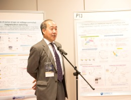
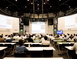
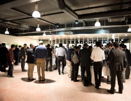
▲ 会場風景

| 9:00-9:40 | Integrated technologies for CMOS/MTJ hybrid nonvolatile micro-controller unit (MCU) - From IC design tool & IP library to process technologies - | |
|---|---|---|
| Prof. Tetsuo Endoh | Tohoku University, Japan | |
| 9:40-10:20 | Spin-orbit torque switching for high-speed nonvolatile memory applications | |
| Prof. Shunsuke Fukami | Tohoku University, Japan | |
| 10:20-11:00 | VOLTAGE-CONTROL SPINTRONICS MEMORIES HAVING A POTENTIAL OF ULTRA-LOW ENERGY CONSUMPTION AS HIGH-DENSITY AND HIGH-SPEED WORKING MEMORIES | |
| Dr. Hiroaki Yoda | Toshiba, Japan | |
| 11:00-11:40 | Voltage controlled magnetic anisotropy through magnetic dipole term induction | |
| Prof. Shinji Miwa | Osaka University, Japan | |
| 11:40-12:20 | New spintronic materials for magnetic tunnel junctions | |
| Dr. Kazuhiro Hono | NIMS, Japan | |
| 12:30-13:10 | STT-MRAM: ON THE CUSP OF MASS PRODUCTION | |
|---|---|---|
| Dr. Yiming Huai | Avalanche Technology, USA | |
| 13:10-13:50 | Perpendicular STT-MRAM as an Emerging Embedded Non-volatile Memory with Data Retention through Solder Reflow Processing | |
| Dr. William J. Gallagher | TSMC, Taiwan | |
| 15:00-15:40 | Phase Change Memory with Topological Functionalities | |
|---|---|---|
| Dr. Junji Tominaga | AIST, Japan | |
| 15:40-16:20 | Applications of Emerging Nonvolatile Memory in Future Intelligent Storage and Computing | |
| Prof. Yiran Chen | Duke University, USA | |
| 16:20-17:00 | Fast, low-current spin-orbit switching of magnetic tunnel junctions using Hf interface engineering | |
|---|---|---|
| Dr. Yongxi Ou | Cornell University, USA | |
| 17:00-17:40 | Unconventional spin-orbit torques and their applications | |
| Prof. Hyunsoo Yang | National University of Singapore, Singapore | |
| 17:40-18:20 | Electric Field and Strain Control of Magnetism: Towards Ultralow Energy Memory Devices | |
| Prof. Nicholas G. Kioussis | California State University Northridge, USA | |
| 18:20 | Closing (Day2) | |
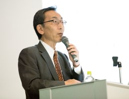
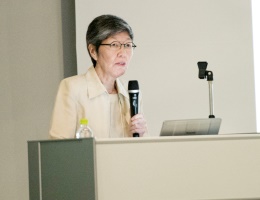
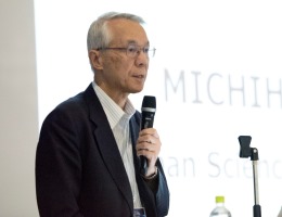
▲ 大野分科会会長(東北大学)

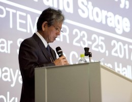
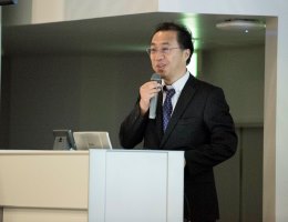
▲ 湯浅分科会会長(産総研)
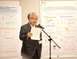
▲ 会場風景

| 9:00-9:15 | Dr. Tomio Suzuki | Cabinet Office, Government of Japan |
|---|---|---|
| 9:15-9:30 | Mr. Atsuo Hirai | Ministry of Economy, Trade and Industry |
| 9:30-9:45 | Prof. Hirotsugu Takizawa | Tohoku University, Japan |
| 9:45-10:25 | Spintronics: A Potential Pathway to Enable an Exponential Scaling for the Beyond-CMOS Era | |
|---|---|---|
| Prof. Jian-Ping Wang | Minnesota University, USA | |
| 10:25-11:05 | Roadmap of low dissipation spintronics technology | |
| Prof. Kang L. Wang | UCLA, USA | |
| 11:05-11:45 | Project for Development of Next-Generation Smart Devices
- Development of over 1,000 GOPS/W Image Recognition Processor Platform Technologies - |
|
|---|---|---|
| Dr. Masahiro Nomura | Renesas Electronics, Japan | |
| 12:00-12:40 | Advanced Manufacturing Technologies for STT-MRAM | |
|---|---|---|
| Dr. Hiroki Maehara | Tokyo Electron, Japan | |
| 13:30-14:10 | Neuromorphic device for Cognitive Computing | |
|---|---|---|
| Dr. Shintaro Yamamichi | IBM, Japan | |
| 14:10-14:50 | Towards a new computing paradigm | |
| Dr. Yasunori Kimura | Fujitsu, Japan | |
| 14:50-15:30 | Social Value Creation Accelerated by Heterogeneous Computing and Spintronics | |
| Dr.Yuichi Nakamura | NEC, Japan | |
| 15:40 | 2016year Best Poster Award Ceremony and Closing Remarks, “See you next year in Tokyo” (Day 3) | |
▲ Greeting 鈴木参事官(Cabinet Office)
▲ Greeting 平井課長(METI)

▲ Greeting 滝澤研究科長(東北大学)

▲ 会場風景

| 01 | Outline of ImPACT Sahashi Program Masashi Sahashi (Program Manager, Tohoku Univ.) |
|---|---|
| 02 | Spintronic Integrated Circuit Project H. Ohno, T. Endoh, T. Hanyu, S. Ikeda (Tohoku Univ.) |
| 03 | Scheme of ImPACT Voltage-Torque MRAM Project S. Yuasa(AIST) |
| 04 | Simulation Support Team H. Imamura1, M. Shirai2, T. Oda3, K. Nakamura4, Y. Miura5 (1AIST, 2Tohoku Univ, 3Kanazawa Univ, 4Mie Univ, 5KIT) |
| 05 | Effect of CoFeB composition on magnetic and free-layer properties of MgO/(Co)FeB/MgO structure M. Bersweiler, H. Sato, H. Ohno (Tohoku Univ.) |
| 06 | Quantifying Dzyaloshinskii-Moriya interaction from thermally-activated and flow regime domain wall dynamics S. DuttaGupta, C. Zhang, S. Fukami, H. Ohno (Tohoku Univ.) |
| 07 | Coercivity dependent on magnetic-field-angle in a nanoscale CoFeB-MgO magnetic tunnel junction with perpendicular easy axis J. Igarashi, J. Llandro, H. Sato, H Ohno (Tohoku Univ.) |
| 08 | Spin-orbit torque driven magnetization reversal in Co/Pt multilayer B. Jinnai, C. Zhang, A. Kurenkov, M. Bersweiler, H. Sato, S. Fukami, H. Ohno (Tohoku Univ.) |
| 09 | Spin-orbit torque-induced magnetization reversal in nanoscale W/CoFeB/MgO prepared with various tungsten sputtering conditions C. Zhang, S. Fukami, K. Watanabe, A. Ohkawara, S. DuttaGupta, H. Sato, F. Matsukura, H. Ohno (Tohoku Univ.) |
| 10 | Energy-Efficient Data-Access Technique for an Ultra Low-Power Nonvolatile Microcontroller Unit M. Natsui, T. Hanyu (Tohoku Univ.) |
| 11 | Design of a Multi-Functional MTJ-Based FPGA for an Ultra-Low-Power Microcontroller Unit D. Suzuki, T. Hanyu (Tohoku Univ.) |
| 12 | Development of integrated circuit and 300 mm integrated process for spintronic integrated circuit T. Endoh, S. Ikeda, H. Koike, Y. Noguchi, H. Ohno (Tohoku Univ.) |
| 13 | Cr doping effect on interfacial magnetic anisotropy and voltage-controlled magnetic anisotropy at the Fe/MgO interface T. Nozaki1, A. Kozioł-Rachwał1,2, S. Tamaru1, H. Kubota1, A. Fukushima1, Y. Suzuki1,3, S. Yuasa1 (1AIST, 2AGH Univ., 3Osaka Univ) |
| 14 | Effects of pulse shape on voltage-controlled magnetization switching T. Yamamoto1, Y. Shiota1, T. Nozaki1, T. Ikeura1,2, S. Tamaru1, K. Yakushiji1, H. Kubota1, A. Fukushima1, Y. Suzuki1,3, S. Yuasa1 (1AIST, 2Tsukuba Univ., 3Osaka Univ.) |
| 15 | Fabrication of a fully epitaxial magnetic tunnel junction on an 8 inch Si wafer A. Sugihara, K. Yakushiji, S. Yuasa (AIST) |
| 16 | Three-dimensional Integration of Perpendicular-type Magnetic Tunnel Junctions for STT-MRAM Application K. Yakushiji, H. Takagi, N. Watanabe, A. Fukushima, K. Kikuchi, Y. Kurashima, A. Sugihara, H. Kubota, S. Yuasa (AIST) |
| 17 | Fabrication of Magnetic Tunnel Junctions with below 20nm diameter A. Fukushima, A. Sugihara, K. Yakushiji, H. Kubota, S. Yuasa (AIST) |
| 18 | Toward giant tunnel magnetoresistance in (001) epitaxial magnetic tunnel junctions using spinel oxides M. Belmoubarik, H. Sukegawa, T. Scheike, T. Ohkubo, S. Mitani, K. Hono (NIMS) |
| 19 | Development of magnetic tunnel junctions with chalcopyrite-type compound semiconductor barriers K. Mukaiyama, S. Kasai, J. Wang, Y. K. Takahashi, S. Mitani, K. Hono (NIMS) |
| 20 | Low-temperature measurements of voltage-controlled magnetic anisotropy in Cr/Fe/MgAl2O4 M. Al-Mahdawi, Q. Xiang, M. Belmoubarik, H. Sukegawa, S. Kasai, S. Mitani, K. Hono (NIMS) |
| 21 | Effect of material selection on bonding interface for direct wafer bonding processing of epitaxial magnetoresistive devices J. Chen1,2, Y. Sakuraba2 , K. Yakushiji3, H. Takagi3, Y. Kurashima3, N. Watanabe3, K. Kikuchi3, S. Yuasa3, K. Hono1,2 (1Univ. of Tsukuba, 2NIMS, 3AIST) |
| 22 | Voltage control of perpendicular magnetic anisotropy in Fe/MgAl2O4 heterostructures: significant effect of the Fe atomic layer numbers Q. Xiang1,2, H. Sukegawa1, M. Al-Mahdawi1, M. Belmoubarik1, S. Kasai1, Y. Sakuraba1, S. Mitani1,2, K. Hono1,2 (1NIMS, 2Univ. of Tsukuba) |
| 23 | Perpendicular magnetic tunnel junctions using ultra-thin Mn-based electrodes K. Z. Suzuki1, R. Ranjbar1, L. Bainsla1, A. Ono1, Y. Sasaki1,3, Y. Miura2, S. Mizukami1 (1WPI-AIMR, 2KIT, 3Tohoku Univ.) |
| 24 | In-plane current-induced switching in Mn-based storage layer for perpendicular magnetic tunnel M. Takikawa1,2, K. Z. Suzuki1, R. Ranjbar1, S. Mizukami1 (1WPI-AIMR, 2Tohoku Univ.) |
| 25 | Electric field effect on magnetic anisotropy at Fe1-xCoxPd/MgO interface A. K. Shukla1, M. Goto1,2, K. Nawaoka1, J. Suwardy1, S. Miwa1,2, Y. Suzuki1,2 (1Osaka Univ., 2CSRN Osaka Univ.) |
| 26 | Microscopic origin of voltage-controlled magnetic anisotropy in ferromagnetic thin-film metals S. Miwa1,6, M. Suzuki2, M. Tsujikawa3,7, T. Nozaki4, T. Tsukahara1, T. Kawabe1, K. Yoshikawa1, K. Nawaoka1, M. Goto1,6, Y. Kotani2, K. Toyoki2, T. Nakamura2, T. Ohkubo5, K. Hono5, M. Shirai3,7, S. Yuasa4, Y. Suzuki1,6 (1Osaka Univ., 2JASRI, 3Tohoku Univ., 4AIST, 5NIMS, 6CSRN Osaka Univ., 7CSRN Tohoku Univ.) |
| 27 | EXAFS analysis of an Fe/Pt/MgO junction to study the voltage-induced effects in the interfacial atomic structure M. Suzuki1, T. Tsukahara2, R. Miyakaze2, T. Furuta2, K. Shimose2, M. Goto2,3, T. Nozaki4, S. Yuasa4, Y. Suzuki2,3,4, S. Miwa2,3 (1JASRI, 2Osaka Univ., 3CSRN Osaka Univ., 4AIST) |
| 28 | Voltage-Control Spintronics Memory (VoCSM); memory with low energy consumption in high-speed writing Y. Ohsawa1, H. Yoda1, N. Shimomura1, M. Shimizu1, S. Shirotori1, B. Altansargai1, H. Sugiyama1, K. Koi1, Y.Kato1, T. Inokuchi1, Y. Saito1, S. Oikawa1, M. Ishikawa1, T. Ajay1, T. Sasaki2, T. Ohkubo2, K. Hono2, A. Kurobe1 (1Toshiba, 2NIMS) |
| 29 | Switching Mechanism Design for High-speed Voltage-Control Spintronics Memory (VoCSM) Considering the Operation Window K. Koi, H. Yoda, N. Shimomura, T. Inokuchi, Y. Kato, B. Altansarga¬i , S. Shirotori, Y. Kamiguchi, K. Ikegami, S. Oikawa, H. Sugiyama, M. Shimizu, M. Ishikawa, T. Ajay, Y. Ohsawa, Y. Saito, A. Kurobe (Toshiba) |
| 30 | Voltage-controlled magnetic tunnel junction based MRAM for replacing high density DRAM circuits corresponding to 2X nm generation K. Ikegami1, Y. Shiota2, T. Nozaki2, S. Fujita1, S. Yuasa2, Y. Suzuki2,3 (1Toshiba, 2AIST, 3Osaka Univ.) |
| 31 | A 6.75F2/bit Voltage-Control Spintronics Memory Array by Two Memory Layers Stacking and Buried-Wordline Cell Transistors S. Takaya, K. Ikegami, S. Fujita, N. Shimomura, H. Yoda (Toshiba) |
| 32 | Deterministic magnetization switching by voltage controlled Dzyaloshinskii-Moriya interaction H. Imamura, T. Nozaki, S. Yuasa, Y. Suzuki (AIST) |
| 33 | Huge voltage-induced magnetic anisotropy change in the 5d-transtion metal monolayer on the Fe and Co surface M. Tsujikawa1,2, M. Shirai1,2 (1REIC, 2CSRN Tohoku Univ.) |
| 34 | Sign change in the voltage-control magnetic anisotropy in terms of interface electronic structure; thickness and strain effects T. Oda, T. Kanagawa, I. Pardede, N. Ikhsan, M. Obata (Kanazawa Univ.) |
| 35 | Material design of Fe/MgO interfaces for electric-field-modification of magnetocrystalline anisotropy T. Nomura, K. Nakamura (Mie Univ.) |
| 36 | A first-principles study on voltage dependence of interfacial magnetic properties of Fe layer Y. Miura1,2 (1KIT, 2NIMS) |
▲ 伊藤理事(東北大学)
▲ 滝澤研究科長(東北大学)
▲ 会場風景

総数170名
(日本国内 156名、国外(4カ国) 14名(アメリカ8名、フランス1名、台湾3名、シンガポール2名)
●主な一般参加者ご所属一覧 約25機関が参加:
アドバンテスト、インテル、KEYSIGHT TECHNOLOGIES、京都大学、Samsung、SUMCO、ソシオネクスト、ソニー、田中貴金属、TDK、TEL、東京工業大学、東京大学、東北大学、東芝、デンソー、日新イオン機器、日産化学工業、日立製作所、フルヤ金属、北海道大学、ルネサスエレクトロニクス、JST、Avalanche Technology、TSMC 他
Organized by [ImPACT] SAHASHI program, Japan Science and Technology Agency
Copyright © 2017 Japan Science and Technology Agency. All Rights Reserved.