
[本文]
Objective
This program aims to form a globally competitive Super Cluster through wide-range collaboration in order to create innovation with high-impact in our country. While exploiting the achievements of science and technology promotion measures in each area thus far, the government will initiate selection and concentration, finding the best match, based on social and market needs.
Management by SDs [Strategy Directors]
Each Core Cluster establishes an SD team with three SDs (Strategy Directors).
Under their strong leadership, including deciding the budget allocation, they control the management of Super Clusters based on clear management policies and market acquisition plans.
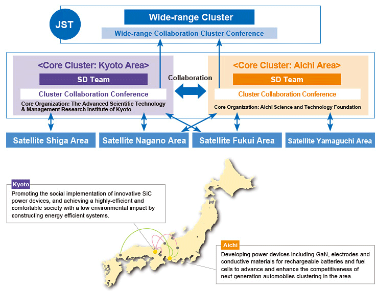
Super Cluster Cooperation Beyond Regions
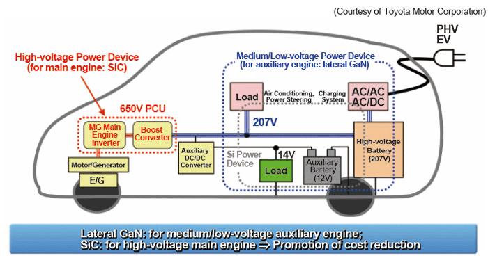
Power Electronics
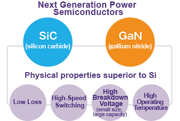
■ SiC (silicon carbide)
In a SiC, half of the silicon material is replaced with carbon. By combining carbon, it allows a robust crystalline figure to be created, thus having a more precise and stable crystal compared to silicon.
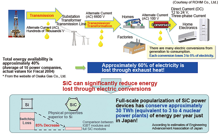
This enables a low loss, high breakdown voltage device to be created, compared to conventional silicon devices.
⇒SiC device has an advantage in high breakdown voltage/ high power applications, such as in motor drive applications.
■ GaN (gallium nitride)
GaN shows more connective stability, and has an even higher critical electric field for breakdown than SiC.
It is also a material used for blue LEDs.
Today, forming a GaN active layer on silicon substrate has become the standard.
⇒ GaN device has the advantage in compact, high frequency applications, such as in switching power supply.