link to move in the page.
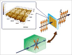
We are exploring plasma photonics to develop advanced functional devices made of high energy density plasmas created by ultra-intense laser light. The plasma photonic devices are realized by coherently and transiently controlling the high energy density plasmas. The advantage of the plasma photonic devices is direct control of high energy density particles as well as intense light with high damage tolerance, which are extremely promising in view of innovative applications in scientific, technological and medical areas.
| Kiminori Kondo | OSAKA UNIVERSITY | Graduate School of Engineering, Department of Electrical Electronic and Information Engineering | Associate Professor |
|---|---|---|---|
| Hitoki Yoneda | University of Electro-Communications | Institute for Laser Science | Associate Professor |
| Noboru Yugami | Utunomiya University | Department of Electrical and Electoronic Engineering, | Professor |
We propose and demonstrate "active meso-optics", a novel method tocontrol light via the dynamical control of the morphology of materials. We examine mechanisms to enhance the unique optical effects caused by a non-local response and/or macroscopic coherence in a material, which aresensitive to a spatial modulation at a sub-wavelength scale. Novel methods to obtain an accurate control of the spatial and temporal profiles of light pulses are also investigated and utilized for a dynamical control of morphology. We also explore novel aspects of light-matter interaction in order to obtain schemes for the active control of light in the visible and THz spectral regions.
| Kazuhiko Misawa | Tokyo University of Agriculture and Technology | Institute of Symbiotic Science and Technology Strategic Research Initiative for Future Nano-science and Technology | Professor |
|---|
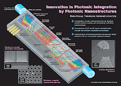
Passive technologies for photonic nanostructures have greatly advanced in these years. In this study, we investigate active optical and photonic phenomena in these structures. Particularly we focus on slowlight generation, efficient optical amplifier, negative refraction, nonlinearity enhancement, and dynamic effects in photonic crystals, and their applications to functional devices. We integrate these devices with silicon photonics to provide a breakthrough technology for photonic integration and signal processing.
| Masaya Notomi | NTT Basic Research Laboratories | Photonic Nanostructure Group | Group Leader |
|---|
To advance the information society, the development of high-capacity, cost-effective optical communications systems is desired. For this purpose, as a light source, a laser diode with temperature stability is needed. We have found that InN, a component of nitride semiconductors used in blue LEDs, emits infrared light whose wavelength is stable against temperature change. This laser has environmental advantages because it does not contain arsenic or phosphor. This project seeks to fabricate laser diodes with an InN emitting layer for optical communications systems.
| Hideo Nakae | Waseda University | Department of Materials Science and Engineering School of Science and Engineering / Materials Science and Engineering | Professor |
|---|---|---|---|
| Shiyoshi Yokoyama | National Institute of Information and Communications Technology | ICT Research Center | Senior resercher |
| Akiko GOMYO | NEC | Nano Electronics Research Laboratories | Principal Principle Investigators |
Electrons in some transition metal oxides and complexes mutually interact strongly so that their independent motion is suppressed. This is called electron correlation. The correlation brings about spontaneous order among the electrons. The electron ordering is strongly affected by light and light, in turn, is strongly modulated by the electron order. In this way, light and the electron order are tightly bound and bilaterally controllable. In this project, we will optimize and maximize the light-electron interaction through artificial structures so that even electrons in a single lattice layer can produce profound effects.
| Hiroshi Okamoto | The University of Tokyo | Department of Advanced Materials Science Graduate School of Frontier Science | Professor |
|---|
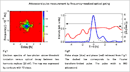
Sub-100 attosecond, soft Xray pulses and optical field shapes on demand are achieved by combining the advanced high power laser technology with the precise optical synthesizing. "An attosecond oscilloscope" is developed by using a 100-attosecond pulses as a pump and trigger, and a saw tooth optical field as a sweep. With this system, the high-speed electron motion induced by Auger process and chemical reaction is recorded as continuous snap shots. In addition, the technique to steer electron motion in materials on an attosecond time scale is developed towards the verification of a new function.
| Kenji Toritsuka | National Institute of Advanced Industrial Science and Technology | Photonics Research Institute | Group Leader |
|---|