- JST Home
- /
- Strategic Basic Research Programs
- /
 ERATO
ERATO- /
- Research Area/Projects/
- Completed/
- OHTSU Localized Photon
OHTSU Localized Photon

Research Director: Dr. Motoichi Ohtsu
(Professor, Interdisciplinary Graduate School of Science and Engineering, Tokyo Institute of Technology)
Research Term: 1998-2003
A novel optical nano-technology that exceeds the diffraction limit is required to support future optical science and technology. To meet this requirement, this project has studied nanophotonics (a technology to fabricate and operate nanometric photonic devices, which utilize local electromagnetic interactions between a small nanometric element and an optical near field) and atom-photonics (a technology of manipulates atoms by using an optical near field), together with the nature of optical near fields theoretically. A quantum mechanics theory of optical near fields has been developed. A nanophotonic switch and related devices have been developed. Nanofabrications (e.g., photochemical vapor deposition) using optical near fields were developed. For atom manipulation using an optical near field, optical near field devices have been developed for atom deflection, trapping, and detection. This project has been highly successful from both theoretical and practical perspectives. Not only is the basic concept of the optical near field much better understood, but a wide variety of concepts and applications have been proposed and demonstrated. These results have stimulated very great interest in a surprisingly wide range of technology, including optical fiber communications and optical information processing, optical sensing, optical storage, input/output interfaces and display systems.
Research Results
Optical near field theory
Quantum theory of an optical near-field system :
The theory group has developed a quantum theory of an optical near-field system that consists of a nanometric material-probe tip system connected to a macroscopic material system, such as a fiber-probe body or substrate, via incident photons. Phenomena and quantum mechanical observables that are difficult for conventional optical near-field theories to handle are being investigated. This approach is unique, both from the viewpoint of basic theory on optical near-fields and in application to nano and atom photonics. While developing an intuitive model, we have tried to analyze critical issues related to nanofabrication and the realization of nanophotonic devices, and we continue to explore new principles concerning the operation of such devices and single atom manipulation (deflection/trap), in collaboration with other experimental groups involved in this project. We have also compared our theoretical results with experimental data and with results obtained using other theories, where possible, in order to obtain feedback and to strengthen our approach.
In the first half of the project period, we concentrated on formulating a steady state using a projection operator method. We derived an effective optical near-field interaction between a nanometric material system and a probe tip system, which is expressed in terms of the Yukawa function with a finite interaction range. Based on the effective optical near-field interaction, we proposed an intuitive, phenomenological model – the localized photon model.
In the second half of the project period, using these two models and solving the quantum master equation or the Heisenberg equation, we predicted a novel mechanism and the dynamics that are inherent in an optical near-field system, but which are difficult to obtain by propagating a far field. For example, we predicted the occurrence of dipole ordering of a nanometric quantum dot system as a collective phenomenon, numerically showing the importance of local manipulation of the initial conditions that lead to dipole ordering and superradiance, which is emitted from the dipole-ordered state. We proposed a nanophotonic switch using a three-quantum-dot system coupled by an optical near-field, and analyzed the exciton dynamics of the system in order to estimate the properties of the device, including a switching time that proved consistent with experimental results obtained by the nanophotonics group. We also examined a logic device, based on a quantum dot system coupled via an optical near-field, as an application of the unique dynamics of optical near-field systems.
To fabricate such elements of nanophotonic devices while controlling the size and position of each component, we analyzed fundamental issues concerning atom/molecule manipulation using optical near-fields, and predicted the possibility of developing a single atom trap using an optical near-field probe tip. We also suggested an important mechanism for nanofabrication, which uses molecular dissociation with an optical near-field.
Nanophotonics
Nanophotonic switch:
A nanophotonic switch is proposed by utilizing the dipole forbidden energy transfer that occurs between CuCl quantum cubes (QCs), X and Y, in close proximity, with effective side lengths of 4.6 and 6.3 nm, respectively (Fig. (a)). The quantized exciton energy levels of (1,1,1) in QC X and (2,1,1) in QC Y resonate with each other. With this resonance, the optical near-field couples X and Y, allowing energy transfer to occur between the QCs via the optical near-field. Assuming that the separation between the two QCs is 10 nm, the estimated energy transfer time is 40 ps, which is much shorter than the exciton lifetime and is longer than the inter-sub-level transition time. Therefore, most of the excitons in the 4.6-nm CuCl QC transfer to the neighboring 6.3-nm QC. Here, we note that this energy transfer is optically forbidden owing to optically inactive features of the energy level (2,1,1), but is possible with optical near-fields because of the steep spatial gradient of the field intensity.
Photoluminescence images of luminescence from QCs with side lengths of 4.6 and 6.3 nm clearly show the anti-correlation features in their intensity distributions as shown in Fig. (b) and (c). This anti-correlation feature is explained by the energy transfer from X cubes to Y cubes. Namely, a 4.6-nm QC located close to a 6.3-nm QC cannot emit light, but instead transfers energy to the 6.3-nm QC. As a result, the luminescence intensity from the 4.6-nm QC is low, while that from the 6.3-nm QC is high. The experimentally measured energy transfer time agreed well with the value estimated theoretically.
Nanophotonic waveguide:
To connect nanophotonic devices with conventional diffraction-limited photonic devices, it is necessary to convert far-field light to an optical near-field. A plasmon waveguide has been proposed as a converter, by introducing a metal-coated silicon wedge structure. The guiding characteristics of a plasmon waveguide fabricated using the Si anisotropic etching process were determined to have a 150-nm beam width and a propagation length exceeding several microns.
Fabrication of nanometric materials:
To achieve nanometric accuracies in sizes and positions of the nanophotonic devices, we first showed the feasibility of using optical near-field techniques for nanometer-scale CVD by demonstrating highly controlled deposition of 60-nm Zn dots. To fabricate even smaller dots, we demonstrated deposition of nanometer-scale Zn dots, using selective photodissociation of adsorbed diethylzinc (DEZn) molecules, in which the photon energy is lower than that of the absorption edge of gas-phase DEZn. We achieved nanometric prenucleation by dissociating the DEZn molecules adsorbed on a substrate. Subsequent deposition resulted from dissociating the adsorbed molecules on prenucleated Zn. The topographic image of the deposited Zn dot had a full width at half maximum of 25 nm. In the quest to further control size, we reported that illumination with a nonresonant optical near-field, which does not dissociate DEZn molecules, dramatically influences and regulates the growth of Zn nanoparticles during NFO-CVD. In this deposition, the dependency of fabricated dot size on photon energy is due to size-dependent resonance during optical absorption. We also discussed the possibility of applying this technique to self-assembly fabrication, for the mass production of nanophotonic ICs. Since these methods can be used for a variety of nanomaterials, they are a promising tool for nanophotonics.
Optical CVD utilizes a two-step process: photodissociation and adsorption. For photodissociation, far-field light must resonate the reacting molecular gases in order to excite molecules from the ground state to an excited electronic state. The Frank-Condon principle states that this resonance is essential for excitation. The excited electron state of the usual metal-organic gas source for optical CVD is in the ultraviolet region. For NFO-CVD, however, photodissociation can take place under non-resonant conditions, i.e., using visible light, due to the inherent properties of optical near-fields; using an optical near-field, photodissociation and deposition occur even with non-resonant light. We also discussed the physical mechanisms of this phenomenon using photon energy and light intensity dependence. These phenomena are the first steps on a path that will lead to the fabrication of new optical devices.
In addition to ZnO nanodots, we have also fabricated Si and GaN nanodots using photochemical reactions. These semiconductor nanomaterials extend the possibilities of nanophotonic devices.
Development of functional probes:
A variety of functional probes were developed for application to NFO-CVD and advanced characterization of the use of optical near-fields, including diamond, fluoride-resin-coated fiber, and temperature-controllable Si probes.
Atom-photonics
The atom photonics group has developed atom control techniques that use optical near-field, including atom deflection and a single-atom trap. These techniques will be applied to atom-by-atom deposition and crystal growth, as well as to study of the interaction between atoms and optical near-field.
First, we generated a cold atomic beam that passes through a near-field optical funnel, using cold atoms produced by a magneto-optical trap (MOT). Such cold atomic beams are required for efficient interaction with nanometric optical near-field. In the funnel, Rb atoms that drop from the MOT by gravity are reflected by the repulsive dipole force from the optical near-field induced on the inner-wall surface via total internal reflection of a blue-detuned light beam. We used a probe-light beam to observe multi-reflection of Rb atoms inside the funnel at a temperature of 9 mK owing to polarization gradient cooling. Moreover, when the excitation light beam is blue-detuned with respect to the lower ground state of the hyperfine structure of Rb atoms, the Rb atoms lose their kinetic energy in reflection. This energy loss is repeatable if we use additional pumping light from the upper ground state to the lower ground state (Sisyphus cooling). Indeed, by using a probe light beam we observed the Sisyphus cooling effect by monitoring the increase in the number of atoms that collected at the bottom of the funnel. In order to detect a small number of atoms outside the funnel, we developed an accumulation counting system using the MOT. When the MOT detection system was placed 25 cm below the 200-mm exit hole, the output of Rb atoms was estimated to be 105 atoms/s·cm2 under blue-detuning of 1.2 GHz. To increase the flux density, we also made an atom funnel with a 2.3-mm exit hole. If a hollow-light beam is used to excite near-field light, the flux density is estimated to be 1012 atoms/s·cm2, which was sufficient for the atom-deflection experiment. We generated a hollow-light beam for the funnel using the interference method.
Next, we developed a near-field optical deflector that precisely controlled atomic motion using a dipole force. The deflector was made by photolithography and anisotropic chemical etching of a (100)-oriented silicon-on-insulator substrate. Blue-detuned optical near-field was generated near the edge of a 100-nm-wide slit; it had a spatial distribution of 126 nm at a distance of 10 nm from the top edge. The deflection angle of a Rb atom is a function of the light intensity, frequency detuning, and atomic velocity. We used a blue-detuned hollow-light beam to guide cold Rb atoms from the MOT to a position 26 cm below it. The mean velocity of the guided atoms was estimated to be 6 m/s from time-of-flight measurements using two-step photoionization. Such atoms can be deflected at a large angle. In order to detect the deflected atoms, we developed a slit-type atom detector using optical near-field. A detector with a 70 ´ 100-mm slit was made by photolithography and anisotropic chemical etching of a silicon-on-insulator substrate. From the measured optical near-field distribution induced in the slit with a fiber probe, the spatial resolution was estimated to be almost the same as the slit width. Atoms were selectively counted by two-step photoionization using two-color optical near-field. The detection efficiency was estimated to be 0.25 for a ground-state Rb atom with a velocity of 10 m/s. To increase the detection efficiency, we developed a multi-slit detector with a 50×100 array. Assuming an Rb atomic beam with a mean velocity of 6 m/s and a waist of 500 mm, 15 atoms per second were detected. The stepwise resonant excitation from the 5S state to the 5D state via the 5P state can also be used to detect Rb. In this case, the blue fluorescence of the second D line is monitored for background-free detection. The detection efficiency was estimated to be 0.03
Finally, we developed a fiber probe for trapping single Rb atoms. An atom can be captured near the tip of the fiber probe by balancing the repulsive dipole force from the blue-detuned optical near-field and the attractive van der Waals force from the tip surface. In the case of a L-type three-level atom like Rb, if the light frequency is blue-detuned for both ground states, the atom is trapped in one of the quantized vibration levels produced in the trap potential for the lower ground state, via transfer from an upper ground state with a shallow potential to a lower ground state with a deeper potential. The trap region that roughly equals half the de-Broglie wavelength was numerically estimated to be about 10 nm for a cold Rb atom when the aperture diameter of the fiber probe is 40 nm. Based on the numerical analysis, we made a fiber probe with an aperture of 40 nm; three-step tapering and shortening of the tip were used for high throughput conversion of far-field light coupled to the fiber probe to optical near-field. From probe-to-probe measurements, we confirmed that optical near-field induced near the tip decayed as a Yukawa function with a decay length of 40 nm. In the process of realizing the single-atom trap, we devised an experimental setup for spectroscopy of cold atoms using the fiber probe.
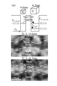
Fig. (a) Schematic explanation of dipole forbidden energy transfer between QCs. (b) and (c) Spatial distributions of the near-field luminescence intensity from QCs with different sizes of L=4.6 nm and L=6.3 nm, respectively.