- JST Home
- /
- Strategic Basic Research Programs
- /
 ERATO
ERATO- /
- Research Area/Projects/
- Completed/
- NISHIZAWA Terahertz
NISHIZAWA Terahertz

Research Director: Dr. Jun-ichi Nishizawa
(President, Tohoku University)
Research Term: 1987-1992
The main theme of this project was to fill in the technological gap between the submillimeter and infrared wavelengths – the tetrahertz (1012 Hz) region – for the further development of telecommunications and processing. The semiconductor devices and circuits studied in this project will most likely find applications in ultra-high-speed integrated circuits, high-density optical-fiber communication systems, plasma diagnostics, remote sensing, radio astronomy and molecular spectroscopy.
Research Results
Photo-stimulated molecular layer epitaxy (PMLE): Methods were developed to fabricate ultra-thin epitaxial gallium arsenide layers of device quality, being controlled to crystal monolayer precision. This method was applied as both a tool and for the development of electron devices.
Semiconductor Raman laser: A semiconductor Raman laser was developed having attractive characteristics for demodulation in the terahertz frequency region as well as a radiation source for the far-infrared wavelength region.
Ideal static induction transistor (ISIT): As a further development of the static induction transistor (SIT), the ISIT features a channel length shorter than the mean-free-path of electrons with atoms of the crystal lattice. The estimated cut-off frequency is around 800 GHz.
TUNNETT diode: Molecular layer epitaxy was applied to fabricate TUNNETT diodes for generators oscillating up to 500 GHz with semi-coaxial cavities.
Schottky barrier diode (SBD): While studying GaAs detectors, mixers, quasi-optical multi-element imaging arrays and frequency multipliers for measurements in the THz region, a fabrication process was developed for low-conversion-loss, low-noise Pt/GaAs Schottky diodes (0.4-0.8µm diameter).
Quasi-optical imaging arrays: Multi-element, quasi-optical imaging arrays consisting of Yagi antennas and Schottky diodes were developed.
Coherent power combiner: To solve the problem of low power generated at very high frequencies, a coherent power combiner was developed. Together with active elements, such as Gunn diodes or FETs, it is effective at millimeter and shorter wavelengths.
Optical waveguide modulators: Among the important devices used for light transmission, switching and signal processing are optical waveguide modulators. A traveling-wave optical modulator was developed which has the potential of offering a perfect matching of microwave and optical velocities.
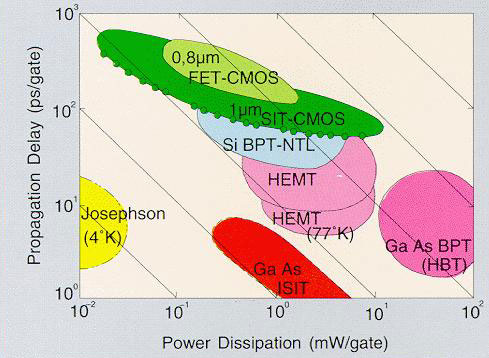
Performance distribution of integrated circuits
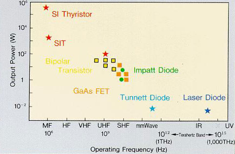
Output power and frequency of semiconductor devices
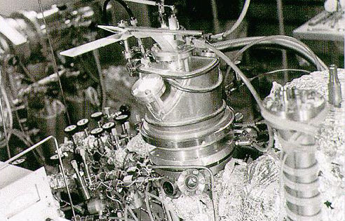
Photostimulated Molecular Layer Epitaxy(PMLE)equipment. This novel method enables the molecular layer single crystal growth of semiconductors such as GaAs,AlxGa1-xAs,lnxGa1-x As and Si with illumination of ultraviolet light.
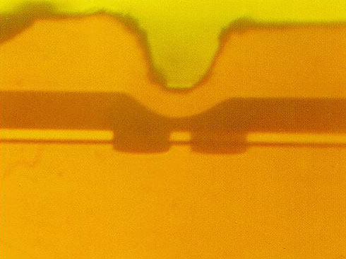
Cross-sectional view of the semiconductor Raman laser