- JST Home
- /
- Strategic Basic Research Programs
- /
 ERATO
ERATO- /
- Research Area/Projects/
- Completed/
- AONO Atomcraft
AONO Atomcraft

Research Director: Dr. Masakazu Aono
(Chief Scientist, RIKEN (Institute of Physical & Chemical Research))
Research Term: 1989-1994
The word “atomcraft” was coined in order to express a new dimension of atomic-scale science and technology in which single-atom manipulation is effectively used. This project carried out systematic studies of the necessary technology and science for manipulating single atoms by the tip of the scanning tunnelling microscope (STM) and while additionally carrying out various related studies.
Research Results
Single-atom extraction: A technique has been developed for routinely extracting single atoms from any predetermined atomic positions using an STM tip, as demonstrated for a silicon surface, Si(111)-(7X7). The physical mechanism of this technique was found to involve a field effect or field evaporation; current effects were found to be negligible.
Binding-energy measurements: It was found that single-atom extraction can be used to directly measure the binding-energy differences of atoms on a given sample surface, as demonstrated on two silicon surfaces, Si(111)-(7X7) and Si(001)-(2X1).
Atom deposition: Atoms of an STM tip can be deposited onto a sample surface, as demonstrated in the combination of a tungsten tip and a silicon sample; however, it is difficult to deposit atoms one by one by this method.
Alternative atom deposition methods: It has been found that one-by-one atom deposition from an STM tip can be achieved by two alternative methods. One is to pick up atoms on an STM tip from a sample surface and to then deposit them one by one at different places on the sample surface. The other method is to deposit atoms one by one from an STM tip is to supply foreign (hydrogen) atoms to the tip (platinum) continuously and to deposit them one by one onto a sample surface (Si(111)-(7X7)).
Atom displacement: A method was found to displace a silicon atom deposited on the Si(111)-(7X7) surface from its original position to another position by the influence of an STM tip at room temperature.
Real-time monitoring system: A technique has been developed to detect/confirm atom extraction and deposition in real time.
Observation of the Coulomb blockade: The Coulomb blockade, which is an important phenomenon in constructing future single-electron tunnelling devices, was observed at room temperature for the first time.
Substrate preparation: A method has been studied for preparing substrate surfaces that are suitable for the atom manipulation by molecular beam epitaxy.
Theoretical studies: In addition to the above, various theoretical studies have been carried out. These include the calculation of STM images, the prediction of stable atomic positions and the interaction between a tip and a sample.
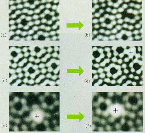
·STM images showing (a)→(b)the extraction of single silicon atom, (c)→(d)the addition of an extra silicon and (e)→(f)the displacement of an extra atom.
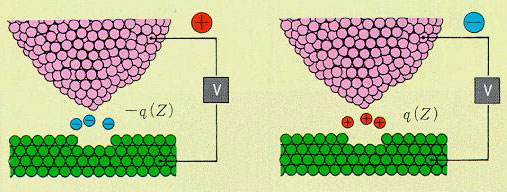
·Schematic figures showing the physical mechanism of the extraction of atoms from the sample surface using an STM tip.
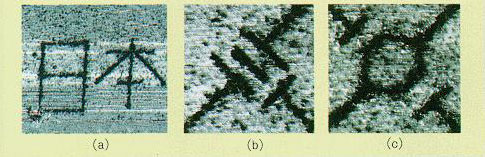
·Characters written on a silicon surface by using the method shown above. (a)Letters;(b)&(c)patterns of the supposed ultramicro-electronic devices. Each pattern has a dimension of about 40nm, 50nm, and 50nm, respectively.